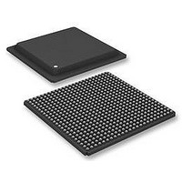
XC6SLX100-2FGG484C Xilinx Inc, XC6SLX100-2FGG484C Datasheet - Page 63

XC6SLX100-2FGG484C
Manufacturer Part Number
XC6SLX100-2FGG484C
Description
FPGA Spartan®-6 Family 101261 Cells 45nm (CMOS) Technology 1.2V 484-Pin FBGA
Manufacturer
Xilinx Inc
Series
Spartan® 6 LXr
Specifications of XC6SLX100-2FGG484C
Package
484FBGA
Family Name
Spartan®-6
Device Logic Cells
101261
Device Logic Units
63288
Number Of Registers
126576
Typical Operating Supply Voltage
1.2 V
Maximum Number Of User I/os
326
Ram Bits
4939776
Number Of Logic Elements/cells
101261
Number Of Labs/clbs
7911
Total Ram Bits
4939776
Number Of I /o
326
Voltage - Supply
1.14 V ~ 1.26 V
Mounting Type
Surface Mount
Operating Temperature
0°C ~ 85°C
Package / Case
484-BBGA
No. Of Logic Blocks
15822
No. Of Macrocells
101261
Family Type
Spartan-6
No. Of Speed Grades
2
No. Of I/o's
326
Clock Management
DCM, PLL
Rohs Compliant
Yes
Lead Free Status / RoHS Status
Lead free / RoHS Compliant
Number Of Gates
-
Lead Free Status / RoHS Status
Lead free / RoHS Compliant
Available stocks
Company
Part Number
Manufacturer
Quantity
Price
Company:
Part Number:
XC6SLX100-2FGG484C
Manufacturer:
ST
Quantity:
4 450
Company:
Part Number:
XC6SLX100-2FGG484C
Manufacturer:
Xilinx Inc
Quantity:
10 000
Table 69: Global Clock Setup and Hold With DCM in System-Synchronous Mode
DS162 (v2.0) March 31, 2011
Preliminary Product Specification
Notes:
1.
2.
3.
Input Setup and Hold Time Relative to Global Clock Input Signal for LVCMOS25 Standard.
T
PSDCM
Setup and Hold times are measured over worst case conditions (process, voltage, temperature). Setup time is measured relative to the Global Clock
input signal using the slowest process, highest temperature, and lowest voltage. Hold time is measured relative to the Global Clock input signal using
the fastest process, lowest temperature, and highest voltage. These measurements include DCM CLK0 jitter.
IFF = Input Flip-Flop or Latch
Use IBIS to determine any duty-cycle distortion incurred using various standards.
Symbol
/ T
PHDCM
No Delay Global Clock and IFF
System-Synchronous Mode
Description
(2)
with DCM in
www.xilinx.com
Spartan-6 FPGA Data Sheet: DC and Switching Characteristics
XC6SLX4
XC6SLX9
XC6SLX16
XC6SLX25
XC6SLX25T
XC6SLX45
XC6SLX45T
XC6SLX75
XC6SLX75T
XC6SLX100
XC6SLX100T
XC6SLX150
XC6SLX150T
Device
–0.18
–0.03
–0.03
–0.01
1.54/
1.54/
1.72/
1.70/
1.79/
1.74/
1.76/
1.86/
1.89/
1.64/
1.69/
1.53/
1.53/
0.06
0.06
0.07
0.11
0.11
0.07
0.09
0.39
0.39
-3
(1)
–0.17
–0.02
–0.02
1.63/
1.87/
1.78/
1.79/
1.84/
1.84/
1.98/
1.98/
1.72/
1.72/
1.62/
1.62/
0.12
0.08
0.00
0.12
0.12
0.08
0.10
0.40
0.40
Speed Grade
N/A
-3N
–0.17
–0.02
–0.02
1.75/
1.75/
2.13/
2.00/
2.00/
2.02/
2.02/
2.20/
2.20/
1.97/
1.97/
1.82/
1.82/
0.12
0.12
0.08
0.00
0.12
0.12
0.08
0.10
0.40
0.40
-2
2.84/
2.84/
2.31/
2.88/
2.64/
2.96/
2.70/
2.75/
0.27
0.27
0.26
0.20
0.52
0.58
0.99
1.00
N/A
N/A
N/A
N/A
N/A
-1L
Units
ns
ns
ns
ns
ns
ns
ns
ns
ns
ns
ns
ns
ns
63


