MJE18008G ON Semiconductor, MJE18008G Datasheet
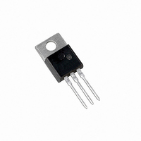
TRANS PWR NPN 8A 450V TO220AB

MJE18008G

Manufacturer Part Number
MJE18008G
Description
TRANS PWR NPN 8A 450V TO220AB
Manufacturer
ON Semiconductor
Series
SWITCHMODE™r
Datasheet

Specifications of MJE18008G

Transistor Type
NPN
Current - Collector (ic) (max)
8A
Voltage - Collector Emitter Breakdown (max)
450V
Vce Saturation (max) @ Ib, Ic
700mV @ 900mA, 4.5V
Current - Collector Cutoff (max)
100µA
Dc Current Gain (hfe) (min) @ Ic, Vce
14 @ 1A, 5V
Power - Max
125W
Frequency - Transition
13MHz
Mounting Type
Through Hole
Package / Case
TO-220-3 (Straight Leads)
Transistor Polarity
NPN
Mounting Style
Through Hole
Collector- Emitter Voltage Vceo Max
450 V
Emitter- Base Voltage Vebo
9 V
Maximum Dc Collector Current
8 A
Power Dissipation
125 W
Maximum Operating Temperature
+ 150 C
Continuous Collector Current
8 A
Dc Collector/base Gain Hfe Min
14
Maximum Operating Frequency
13 MHz
Minimum Operating Temperature
- 65 C
Lead Free Status / RoHS Status
Lead free / RoHS Compliant
Other names
MJE18008GOS

Available stocks

Company
Part Number
Manufacturer
Quantity
Price
Part Number:
MJE18008G
Quantity:
9 850
Part Number:
MJE18008G
Manufacturer:
AMD
Quantity:
560
MJE18008G, MJF18008G
SWITCHMODEt
NPN Bipolar Power Transistor
For Switching Power Supply Applications
die designed for use in 220 V line−operated SWITCHMODE Power
supplies and electronic light ballasts.
Features
Stresses exceeding Maximum Ratings may damage the device. Maximum
Ratings are stress ratings only. Functional operation above the Recommended
Operating Conditions is not implied. Extended exposure to stresses above the
Recommended Operating Conditions may affect device reliability.
1. Pulse Test: Pulse Width = 5 ms, Duty Cycle ≤ 10%.
2. Proper strike and creepage distance must be provided.
MAXIMUM RATINGS
THERMAL CHARACTERISTICS
© Semiconductor Components Industries, LLC, 2010
April, 2010 − Rev. 7
Collector−Emitter Sustaining Voltage
Collector−Base Breakdown Voltage
Emitter−Base Voltage
Collector Current
Base Current
RMS Isolation Voltage (Note 2)
Total Device Dissipation @ T
Derate above 25°C
Operating and Storage Temperature
Thermal Resistance, Junction−to−Case
Thermal Resistance, Junction−to−Ambient
Maximum Lead Temperature for Soldering
Purposes 1/8″ from Case for 5 Seconds
The MJE/MJF18008G have an applications specific state−of−the−art
#E69369
Improved Efficiency Due to Low Base Drive Requirements:
Tight Parametric Distributions are Consistent Lot−to−Lot
Two Package Choices: Standard TO−220 or Isolated TO−220
MJF18008, Case 221D, is UL Recognized at 3500 V
These Devices are Pb−Free and are RoHS Compliant*
High and Flat DC Current Gain h
Fast Switching
No Coil Required in Base Circuit for Turn−Off (No Current Tail)
(for 1 sec, R.H. < 30%, T
Characteristics
Test No. 1 Per Figure 22a
Test No. 1 Per Figure 22b
Test No. 1 Per Figure 22c
Rating
− Continuous
− Peak (Note 1)
− Continuous
− Peak (Note 1)
C
= 25_C
A
MJE18008
MJE18008
MJE18008
MJF18008
MJF18008
MJF18008
= 25_C)
FE
Symbol
Symbol
T
V
V
V
V
R
R
J
I
I
ISOL
P
CEO
EBO
, T
T
CES
CM
BM
I
I
qJC
qJA
C
B
D
L
stg
MJF18008
−65 to 150
Value
1000
4500
3500
1500
0.36
Max
2.78
62.5
450
125
260
9.0
8.0
4.0
8.0
1.0
1.0
16
45
RMS
: File
1
W/_C
_C/W
_C/W
Unit
Unit
Vdc
Vdc
Vdc
Adc
Adc
_C
_C
W
V
1
See detailed ordering and shipping information in the package
dimensions section on page 7 of this data sheet.
*For additional information on our Pb−Free strategy
1
and soldering details, please download the
ON Semiconductor Soldering and Mounting
Techniques Reference Manual, SOLDERRM/D.
2
2
3
3
POWER TRANSISTOR
G
A
Y
WW
ORDERING INFORMATION
45 and 125 WATTS
TO−220 FULLPACK
UL RECOGNIZED
CASE 221A−09
8.0 AMPERES
http://onsemi.com
CASE 221D
1000 VOLTS
TO−220AB
STYLE 1
STYLE 2
= Pb−Free Package
= Assembly Location
= Year
= Work Week
Publication Order Number:
DIAGRAMS
MARKING
MJE18008G
MJF18008G
MJE18008/D
AYWW
AYWW

Related parts for MJE18008G

MJE18008G Summary of contents

Page 1

... MJE18008G, MJF18008G SWITCHMODEt NPN Bipolar Power Transistor For Switching Power Supply Applications The MJE/MJF18008G have an applications specific state−of−the−art die designed for use in 220 V line−operated SWITCHMODE Power supplies and electronic light ballasts. Features • Improved Efficiency Due to Low Base Drive Requirements: High and Flat DC Current Gain h ♦ ...

Page 2

ELECTRICAL CHARACTERISTICS Î Î Î Î Î ...

Page 3

TYPICAL STATIC CHARACTERISTICS 100 T = 125° 25° 20° 0.01 0 COLLECTOR CURRENT (AMPS) C Figure 1. DC Current Gain @ 1 Volt 25°C J ...

Page 4

TYPICAL SWITCHING CHARACTERISTICS 1500 B(off 300 1000 500 ...

Page 5

TYPICAL SWITCHING CHARACTERISTICS 160 150 140 I C 130 120 110 100 25° 125° FORCED ...

Page 6

Figure 18. Dynamic Saturation Voltage Measurements + 100 W 150 ...

Page 7

... SINGLE PULSE 0.01 0.01 0.1 Figure 20. Typical Thermal Response ( 0.5 0.2 0.1 0.1 0.05 0.02 SINGLE PULSE 0.01 0.01 0.1 Figure 21. Typical Thermal Response (Z ORDERING INFORMATION Device MJE18008 MJE18008G MJF18008 MJF18008G TYPICAL THERMAL RESPONSE P (pk DUTY CYCLE TIME (ms) qJC P (pk ...

Page 8

TEST CONDITIONS FOR ISOLATION TESTS* MOUNTED FULLY ISOLATED CLIP PACKAGE LEADS HEATSINK 0.110″ MIN Figure 22a. Screw or Clip Mounting Position for Isolation Test Number 1 *Measurement made between leads and heatsink with all leads shorted together 4-40 SCREW PLAIN ...

Page 9

−B− −Y− 0.25 (0.010 ...

Page 10

... Opportunity/Affirmative Action Employer. This literature is subject to all applicable copyright laws and is not for resale in any manner. PUBLICATION ORDERING INFORMATION LITERATURE FULFILLMENT: Literature Distribution Center for ON Semiconductor P.O. Box 5163, Denver, Colorado 80217 USA Phone: 303−675−2175 or 800−344−3860 Toll Free USA/Canada Fax: 303− ...

Related keywords