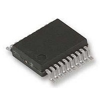
ATA5743P6-TKQY 19 Atmel, ATA5743P6-TKQY 19 Datasheet - Page 21

ATA5743P6-TKQY 19
Manufacturer Part Number
ATA5743P6-TKQY 19
Description
RF Receiver UHF ASK / FSK Receiver
Manufacturer
Atmel
Type
Receiverr
Datasheet
1.ATA5743P3-TGQY.pdf
(43 pages)
Specifications of ATA5743P6-TKQY 19
Package / Case
SSO-20
Operating Frequency
449 MHz
Operating Supply Voltage
4.5 V to 5.5 V
Maximum Operating Temperature
+ 105 C
Minimum Operating Temperature
- 40 C
Mounting Style
SMD/SMT
Noise Figure
7 dB
Lead Free Status / RoHS Status
Lead free / RoHS Compliant
Figure 6-16. Data Clock Disappears Because of a Logical Error
Figure 6-17. Output of the Data Clock After a Successful Bit Check
4839B–RKE–08/05
Dem_out
Data_out (DATA)
DATA_CLK
Dem_out
Data_out (DATA)
DATA_CLK
The delay of the data clock is calculated as follows:
t
t
depends on the capacitive load C
falling edge, t
Figure 6-19 on page 22
level of Data_Out, the data clock is issued after an additional delay t
Note that the capacitive load at pin DATA is limited. If the maximum tolerated capacitive load at
pin DATA is exceeded, the data clock disappears (see section
Delay
Delay1
= t
is the delay between the internal signals Data_Out and Data_In. For the rising edge, t
Delay1
1
1
Receiving mode,
bit check active
Bit check ok
+ t
Delay1
1
1
Delay2
depends additionally on the external voltage V
Receiving mode,
data clock control
logic active
1
1
and
0
1
Figure 6-26 on page
L
1
1
at pin DATA and the external pull-up resistor R
Data
Start bit
Data
1
0
Logical error (Manchester code violation)
Receiving mode,
data clock control
logic active
?
1
29). When the level of Data_In is equal to the
0
1
Receiving mode,
bit check aktive
0
0
“Data Interface” on page
X
(see
1
1
Delay2
Figure 6-18 on page
.
0
0
ATA5743
pup
. For the
29).
Delay1
22,
21


