TR3003 RFM, TR3003 Datasheet - Page 7
TR3003
Manufacturer Part Number
TR3003
Description
RF Receiver 2G ASH Transceiver 303.825MHz 115.2kbps
Manufacturer
RFM
Type
Transceiverr
Datasheet
1.TR3003.pdf
(12 pages)
Specifications of TR3003
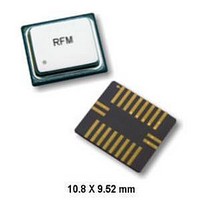
Package / Case
SM-20L
Operating Frequency
304.025 MHz
Operating Supply Voltage
3.3 V
Maximum Operating Temperature
+ 85 C
Minimum Operating Temperature
- 40 C
Mounting Style
SMD/SMT
Lead Free Status / RoHS Status
Lead free / RoHS Compliant


www.RFM.com
©2008 by RF Monolithics, Inc.
The transmitter RF output power is proportional to the input current
to the TXMOD pin. A series resistor is used to adjust the peak
transmitter output power. 1.5 dBm of output power requires about
250 µA of input current.
Transceiver Mode Control
The four transceiver operating modes – receive, transmit ASK,
transmit OOK, and power-down (sleep), are controlled by the
Modulation & Bias Control function, and are selected with the
CNTRL1 and CNTRL0 control pins. Setting CNTRL1 and CNTRL0
both high place the unit in the receive mode. Setting CNTRL1 high
and CNTRL0 low place the unit in the ASK transmit mode. Setting
CNTRL1 low and CNTRL0 high place the unit in the OOK transmit
mode. Setting CNTRL1 and CNTRL0 both low place the unit in the
power-down (sleep) mode. Note that the resistor driving TXMOD
must be low in the receive and power-down modes. The PWIDTH
resistor must also be low in the power down mode to minimize
current. CNTRL1 and CNTRL0 are CMOS compatible inputs.
These inputs must be held at a logic level; they cannot be left
unconnected.
Transceiver Event Timing
Transceiver event timing is summarized in Table 1. Please re-
fer to this table for the following discussions.
Turn-On Timing
The maximum time t
operational at turn on is influenced by two factors. All receiver
circuitry will be operational 5 ms after the supply voltage reaches
2.2 Vdc. The BBOUT-CMPIN coupling-capacitor is then DC
stabilized in 3 time constants (3*t
stable receiver operation for a 10 ms power supply rise time is:
t
The maximum time required for either the OOK or ASK transmitter
mode to become operational is 5 ms after the supply voltage
reaches 2.2 Vdc.
Receive-to-Transmit Timing
After turn on, the maximum time required to switch from receive to
either transmit mode is 12 µs. Most of this time is due to the start-
up of the transmitter oscillator.
Transmit-to-Receive Timing
The maximum time required to switch from the OOK or ASK
transmit mode to the receive mode is 3*t
BBOUT- CMPIN coupling-capacitor time constant. When the
operating temperature is limited to 60
switch from transmit to receive is dramatically less for short
transmissions, as less charge leaks away from the
BBOUT-CMPIN coupling capacitor.
Sleep and Wake-Up Timing
The maximum transition time from the receive mode to the power-
down (sleep) mode t
both low (1 µs fall time).
The maximum transition time from either transmit mode to the
sleep mode (t
are both low (1 µs fall time).
The maximum transition time t
receive mode is 3*t
coupling-capacitor time constant. When the operating temperature
is limited to 60
is dramatically less for short sleep times, as less charge leaks
PR
= 15 ms + 3*t
TOS
o
E-mail: info@rfm.com
BBC
C, the time required to switch from sleep to receive
and t
BBC
PR
RS
required for the receive function to become
, where t
TAS
is 10 µs after CNTRL1 and CNTRL0 are
) is 10 µs after CNTRL1 and CNTRL0
SR
BBC
BBC
from the sleep mode to the
is the BBOUT-CMPIN
). The total turn-on time to
o
C, the time required to
BBC
, where t
BBC
is the
away from the BBOUT- CMPIN coupling capacitor.
The maximum time required to switch from the sleep mode to
either transmit mode (t
due to the start-up of the transmitter oscillator.
AGC Timing
The maximum AGC engage time t
a -30 dBm RF signal with a 1 µs envelope rise time.
The minimum AGC hold-in time is set by the value of the capacitor
at the AGCCAP pin. The hold-in time t
t
Peak Detector Timing
The Peak Detector attack time constant is set by the value of the
capacitor at the PKDET pin. The attack time t
where t
time constant t
Pulse Generator Timing
In the low data rate mode, the interval t
of an ON pulse to the first RF amplifier and the rising edge of the
next ON pulse to the first RF amplifier is set by a resistor R
between the PRATE pin and ground. The interval can be adjusted
between 0.1 and 5 µs with a resistor in the range of 51 K to 2000
K. The value of the R
R
In the high data rate mode (selected at the PWIDTH pin) the
receiver RF amplifiers operate at a nominal 50%-50% duty cycle.
In this case, the period t
first RF amplifier to the start of the next ON pulse to the first RF
amplifier is controlled by the PRATE resistor over a range of 0.1 to
1.1 µs using a resistor of 11 K to 220 K. In this case R
by:
R
In the low data rate mode, the PWIDTH pin sets the width of the
ON pulse to the first RF amplifier t
ground (the ON pulse width to the second RF amplifier t
at 1.1 times the pulse width to the first RF amplifier in the low data
rate mode). The ON pulse width t
0.55 and 1 µs with a resistor value in the range of 200 K to 390 K.
The value of R
R
However, when the PWIDTH pin is connected to Vcc through a 1
M resistor, the RF amplifiers operate at a nominal 50%-50% duty
cycle, facilitating high data rate operation. In this case, the RF
amplifiers are controlled by the PRATE resistor as described
above.
LPF Group Delay
The low-pass filter group delay is a function of the filter 3 dB
bandwidth, which is set by a resistor R
pin. The minimum 3 dB bandwidth f
in kHz, and R
The maximum group delay t
t
AGH
FGD
PR
PR
PW
= 404* t
= 198* t
is in µs, f
is in µs and C
= 404* t
PKA
PRI
PRC
is in µs and C
PW1
LPF
LPF
+ 10.5, where t
PKD
PW
- 8.51, where t
- 18.6, where t
is in kilohms.
in kHz, and R
is given by:
AGC
= 1000*t
PR
STO
is in pF.
PRC
is given by:
PKD
and t
PKA
PRI
FGD
PRC
from the start of an ON pulse to the
is in pF. The Peak Detector decay
is in µs, and R
.
LPF
PW1
STA
is in µs and R
= 1750/f
PW1
AGC
PW1
LPF
) is 16 µs. Most of this time is
in kilohms.
is in µs and R
LPF
PRI
is 5 µs after the reception of
can be adjusted between
AGH
with a resistor R
= 1445/R
LPF
to ground at the LPFADJ
between the falling edge
= C
PR
PR
= 1.21*R
PKA
AGC
is in kilohms
is in kilohms
LPF
= C
PW
/19.1, where
, where f
PKD
is in kilohms
LPF
TR3003 - 4/4/08
PR
PW
PW2
Page 7 of 12
/4167,
, where
is given
to
PR
LPF
is set
is
Related parts for TR3003
Image
Part Number
Description
Manufacturer
Datasheet
Request
R

Part Number:
Description:
ASH RX 115.2 KBPS 433.92 MHZ
Manufacturer:
RFM
Datasheet:

Part Number:
Description:
RFIC TRANCEIVER MULTI-CHANNEL FS
Manufacturer:
RFM
Datasheet:

Part Number:
Description:
ASH TX 115.2 KBPS 433.92 MHZ
Manufacturer:
RFM
Datasheet:
Part Number:
Description:
Filters 1602MHz BW=61MHz
Manufacturer:
RFM
Datasheet:

Part Number:
Description:
RESONATOR, SM3030-6
Manufacturer:
RFM
Datasheet:

Part Number:
Description:
RESONATOR, SM3030-6
Manufacturer:
RFM
Datasheet:

Part Number:
Description:
RESONATOR, SM3030-6
Manufacturer:
RFM
Datasheet:

Part Number:
Description:
RESONATOR, SM5035-4
Manufacturer:
RFM
Datasheet:
Part Number:
Description:
RESONATOR 418MHZ SM5035-4
Manufacturer:
RFM
Datasheet:
Part Number:
Description:
RESONATOR 315 MHZ SMD
Manufacturer:
RFM
Datasheet:

Part Number:
Description:
10-Terminal Ceramic Surface-Mount Case 7 x 5 mm Nominal Footprint
Manufacturer:
RFM [RF Monolithics, Inc]
Datasheet:
Part Number:
Description:
QUAD-BAND GSM850/GSM/DCS/PCS POWER AMP MODULE
Manufacturer:
RFM [RF Monolithics, Inc]
Datasheet:
Part Number:
Description:
402 to 405 MHz Medical Band Front-end Filter
Manufacturer:
RFM [RF Monolithics, Inc]
Datasheet:
Part Number:
Description:
674.03 MHz SAW Resonator
Manufacturer:
RFM [RF Monolithics, Inc]
Datasheet: