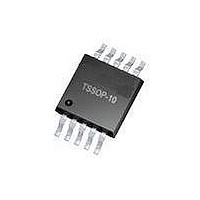
ATA5757-6DQJ Atmel, ATA5757-6DQJ Datasheet - Page 5

ATA5757-6DQJ
Manufacturer Part Number
ATA5757-6DQJ
Description
RF Transmitter ASK/FSK Transmitter 433MHz TPMS
Manufacturer
Atmel
Type
Transmitterr
Datasheet
1.ATAB5756.pdf
(20 pages)
Specifications of ATA5757-6DQJ
Package / Case
TSSOP-10
Operating Frequency
448 MHz
Mounting Style
SMD/SMT
Operating Supply Voltage
2.5 V, 3.3 V
Operating Temperature (min)
-40C
Operating Temperature (max)
125C
Operating Temperature Classification
Automotive
Operating Supply Voltage (typ)
2.5/3.3V
Operating Supply Voltage (max)
3.6V
Lead Free Status / RoHS Status
Lead free / RoHS Compliant
4. Functional Description
4702J–RKE–09/08
The power amplifier is an open-collector output delivering a current pulse which is nearly inde-
pendent from the load impedance and can therefore be controlled via the connected load
impedance.
This output configuration enables a simple matching to any kind of antenna or to 50 Ω. A high
power efficiency for the power amplifier results if an optimized load impedance of
Z
433.92 MHz is used at the 3-V supply voltage.
If ASK = Low, FSK = Low and ENABLE = open or Low, the circuit is in power-down mode con-
suming only a very small amount of current so that a lithium cell used as power supply can work
for many years.
If the ENABLE pin is left open, ENABLE is the logical OR operation of the ASK and FSK input
pins. This means, the IC can be switched on by either the FSK of the ASK input.
If the ENABLE pin is Low and ASK or FSK are High, the IC is in idle mode where the PLL, XTO
and power amplifier are off and the microcontroller ports controlling the ASK and FSK inputs can
be used to control other devices. This can help to save ports on the microcontroller in systems
where other devices with 3-wire interface are used.
With FSK = High and ASK = Low and ENABLE = open or High, the PLL and the XTO are
switched on and the power amplifier is off. When the amplitude of the current through the crystal
has reached 35% to 80% of its final amplitude, the CLK driver is automatically activated. The
CLK output stays Low until the CLK driver has been activated. The driver is activated synchro-
nously with the CLK output frequency, hence, the first pulse on the CLK output is a complete
period. The PLL is then locked within <250 µs after the CLK driver has been activated, and the
transmitter is then ready for data transmission.
With ASK = High the power amplifier is switched on. This is used to perform the ASK modula-
tion. During ASK modulation the IC is enabled with the FSK or the ENABLE pin.
With FSK = Low the switch at pin XTO2 is closed, with FSK = High the switch is open. To
achieve a faster start-up of the crystal oscillator, the FSK pin should be High during start-up of
the XTO because the series resistance of the resonator seen from pin XTO1 is lower if the
switch is off.
The different modes of the ATA5756/ATA5757 are listed in
consumption values can be found in the table
Table 4-1.
ASK Pin
Low
Low
Low
High
High
Low/High
High
Load, opt
= 380 Ω + j340 Ω (ATA5756) at 315 MHz and Z
ATA5756/ATA5757 Modes
FSK Pin
Low
Low
High
Low
High
High
Low/High
ENABLE Pin
Low/open
High
High/open
High/open
High/open
Low
Low
“Electrical Characteristics” on page
Mode
Power-down mode, FSK switch High Z
Power-up, PA off, FSK switch Low Z
Power-up, PA off, FSK switch High Z
Power-up, PA on, FSK switch Low Z
Power-up, PA on, FSK switch High Z
Idle mode, FSK switch High Z
Idle mode, FSK switch High Z
Load, opt
Table
ATA5756/ATA5757
= 280 Ω + j310 Ω (ATA5757) at
4-1, the corresponding current
15.
5


