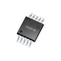
ATA5757-6DQJ Atmel, ATA5757-6DQJ Datasheet - Page 9

ATA5757-6DQJ
Manufacturer Part Number
ATA5757-6DQJ
Description
RF Transmitter ASK/FSK Transmitter 433MHz TPMS
Manufacturer
Atmel
Type
Transmitterr
Datasheet
1.ATAB5756.pdf
(20 pages)
Specifications of ATA5757-6DQJ
Package / Case
TSSOP-10
Operating Frequency
448 MHz
Mounting Style
SMD/SMT
Operating Supply Voltage
2.5 V, 3.3 V
Operating Temperature (min)
-40C
Operating Temperature (max)
125C
Operating Temperature Classification
Automotive
Operating Supply Voltage (typ)
2.5/3.3V
Operating Supply Voltage (max)
3.6V
Lead Free Status / RoHS Status
Lead free / RoHS Compliant
4.4
4.5
4.5.1
4.5.2
4702J–RKE–09/08
Accuracy of the Center Frequency
CLK Output
Clock Pulse Take-over by Microcontroller
Output Matching and Power Setting
The imaginary part of the impedance in large signal steady state oscillation IM
pin 7 (XTO1), causes some additional frequency tolerances, due to pulling of the XTO oscillation
frequency. These tolerances have to be added to the tolerances of the crystal itself (adjustment
tolerance, temperature stability and ageing) and the influence to the center frequency due to tol-
erances of C
should be absorbed into the C
choosing C
quency deviation is as expected. Then, from the nominal value, the IM
using the pulling formula P = -IM
additional frequency tolerance of P = ±16.86 ppm results. If using crystals with other C
additional frequency tolerance can be calculated in the same way. For example, a lower
C
increases the tolerance to 21.07 ppm.
An output CLK signal of 1.64 MHz (ATA5756 operating at 315 MHz) and 1.69 MHz (ATA5757
operating at 433.92 MHz) is provided for a connected microcontroller. The delivered signal is
CMOS-compatible with a High and Low time of >125 ns if the load capacitance is lower than
20 pF. The CLK output is Low in power-down mode due to an internal pull-down resistor. After
enabling the PLL and XTO the signal stays Low until the amplitude of the crystal oscillator has
reached 35% to 80% of its amplitude. Then, the CLK output is activated synchronously with its
output signal so that the first period of the CLK output signal is a full period.
The clock of the crystal oscillator can be used for clocking the microcontroller. Atmel’s ATARx9x
microcontroller family provides the special feature of starting with an integrated RC oscillator to
switch on the ATA5756/ATA5757’s external clocking and to wait automatically until the CLK out-
put of the ATA5756/ATA5757 is activated. After a time period of 250 µs the message can be sent
with crystal accuracy.
The output power is set by the load impedance of the antenna. The maximum output power is
achieved with a load impedance of Z
Z
deliver the DC current (see
The power amplifier delivers a current pulse and the maximum output power is delivered to a
resistive load if the 0.66 pF output capacitance of the power amplifier is compensated by the
load impedance.
At the ANT1 pin, the RF output amplitude is about V
The load impedance is defined as the impedance seen from the ATA5756’s ANT1, ANT2 into
the matching network. Do not mix up this large-signal load impedance with a small-signal input
impedance delivered as an input characteristic of RF amplifiers.
The latter is measured from the application into the IC instead of from the IC into the application
for a power amplifier.
Load, opt
M
= 3.1 fF will reduce the frequency tolerance to 11.87 ppm, where a higher C
= 280 Ω + j310 Ω (ATA5757) at 433.92 MHz. A low resistive path to V
4
and C
4
, C
5
, C
5
, so that the XTO center frequency equals the crystal frequency, and the fre-
Switch
and C
Figure 4-6 on page
4
Stray
and C
XTO
. The nominal value of IM
× C
Load, opt
5
M
values by using a crystal with known frequency and
× π × f
= 380 Ω + j340 Ω (ATA5756) at 315 MHz and
10).
XTO
S
with f
- 0.5 V.
XTO
ATA5756/ATA5757
= 13.56 MHz and C
XTO
= 110 Ω, C
XTO
has ±90 Ω tolerances,
XTO
Switch
S
, seen into the
is required to
M
= 4.4 fF an
and C
M
= 5.5 fF
M
Stray
the
9


