BUB323ZG ON Semiconductor, BUB323ZG Datasheet

TRANS DARL NPN 10A 350V D2PAK

BUB323ZG

Manufacturer Part Number
BUB323ZG
Description
TRANS DARL NPN 10A 350V D2PAK
Manufacturer
ON Semiconductor
Datasheet

Specifications of BUB323ZG

Transistor Type
NPN - Darlington
Current - Collector (ic) (max)
10A
Voltage - Collector Emitter Breakdown (max)
350V
Vce Saturation (max) @ Ib, Ic
1.7V @ 250mA, 10A
Current - Collector Cutoff (max)
100µA
Dc Current Gain (hfe) (min) @ Ic, Vce
500 @ 5A, 4.6V
Power - Max
150W
Frequency - Transition
2MHz
Mounting Type
Surface Mount
Package / Case
D²Pak, TO-263 (2 leads + tab)
Lead Free Status / RoHS Status
Lead free / RoHS Compliant

Available stocks

Company
Part Number
Manufacturer
Quantity
Price
Part Number:
BUB323ZG
Manufacturer:
ON
Quantity:
12 500
Î Î Î Î Î Î Î Î Î Î Î Î
Î Î Î Î Î Î Î Î Î Î Î Î Î Î Î Î Î Î Î
Î Î Î Î Î Î Î Î Î Î Î Î
BUB323Z
NPN Silicon Power
Darlington
High Voltage Autoprotected
D
Darlington with a built−in active zener clamping circuit. This device is
specifically designed for unclamped, inductive applications such as
Electronic Ignition, Switching Regulators and Motor Control.
Features
Maximum ratings are those values beyond which device damage can occur.
Maximum ratings applied to the device are individual stress limit values (not
normal operating conditions) and are not valid simultaneously. If these limits are
exceeded, device functional operation is not implied, damage may occur and
reliability may be affected.
MAXIMUM RATINGS
THERMAL CHARACTERISTICS
© Semiconductor Components Industries, LLC, 2005
August, 2005 − Rev. 1
Collector−Emitter Sustaining Voltage
Collector−Emitter Voltage
Collector Current − Continuous
Base Current
Total Power Dissipation
Operating and Storage Junction
Thermal Resistance, Junction−to−Case
Thermal Resistance, Junction−to−Ambient
Maximum Lead Temperature
The BUB323Z is a planar, monolithic, high−voltage power
2
Over the −40°C to +125°C Temperature Range
Ignition Circuit
Specified Over Full Temperature Range
Integrated High−Voltage Active Clamp
Tight Clamping Voltage Window (350 V to 450 V) Guaranteed
Clamping Energy Capability 100% Tested in a Live
High DC Current Gain/Low Saturation Voltages
Design Guarantees Operation in SOA at All Times
Pb−Free Packages are Available
@ T
Derate above 25_C
Temperature Range
for Soldering Purposes,
1/8 in from Case for 5 Seconds
PAK for Surface Mount
C
= 25_C
Characteristic
Rating
− Peak
− Continuous
− Peak
Î Î Î Î
Î Î Î Î
Î Î Î Î
Î Î Î Î
Î Î Î Î
Î Î Î Î
Î Î Î Î
Î Î Î Î
Î Î Î Î
Î Î Î Î
Î Î Î Î
Î Î Î Î
Î Î Î Î
Î Î Î Î
Î Î Î Î
Î Î Î Î
Î Î Î Î
Î Î Î Î
Î Î Î Î
Î Î Î Î
Î Î Î Î
Î Î Î Î
Î Î Î Î
Î Î Î Î
Î Î Î Î
Symbol
Symbol
T
V
V
R
R
J
I
I
P
, T
CEO
EBO
CM
T
I
I
BM
qJC
qJA
C
B
D
L
stg
Î Î Î
Î Î Î
Î Î Î
Î Î Î
Î Î Î
Î Î Î
Î Î Î
Î Î Î
Î Î Î
Î Î Î
Î Î Î
Î Î Î
Î Î Î
Î Î Î
Î Î Î
Î Î Î
Î Î Î
Î Î Î
Î Î Î
Î Î Î
Î Î Î
Î Î Î
Î Î Î
Î Î Î
Î Î Î
−65 to
Value
+175
Max
62.5
350
150
260
6.0
3.0
6.0
1.0
1.0
10
20
Î Î Î
Î Î Î
Î Î Î
Î Î Î
Î Î Î
Î Î Î
Î Î Î
Î Î Î
Î Î Î
Î Î Î
Î Î Î
Î Î Î
Î Î Î
Î Î Î
Î Î Î
Î Î Î
Î Î Î
Î Î Î
Î Î Î
Î Î Î
Î Î Î
Î Î Î
Î Î Î
Î Î Î
Î Î Î
1
W/_C
_C/W
_C/W
Unit
Unit
Vdc
Vdc
Adc
Adc
_C
_C
W
See detailed ordering and shipping information in the package
dimensions section on page 6 of this data sheet.
360−450 VOLTS CLAMP
ORDERING INFORMATION
AUTOPROTECTED
DARLINGTON
http://onsemi.com
BUB323Z = Specific Device Code
A
Y
WW
G
10 AMPERES
150 WATTS
CASE 418B
STYLE 1
D
2
PAK
CLAMP
360 V
Publication Order Number:
= Assembly Location
= Year
= Work Week
= Pb−Free Package
MARKING
DIAGRAM
BUB323ZG
AYWW
BUB323Z/D

Related parts for BUB323ZG

BUB323ZG Summary of contents

Page 1

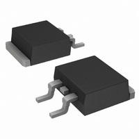
... AUTOPROTECTED DARLINGTON 10 AMPERES 360−450 VOLTS CLAMP 150 WATTS 360 V CLAMP MARKING DIAGRAM BUB323ZG AYWW 2 D PAK CASE 418B STYLE 1 BUB323Z = Specific Device Code A = Assembly Location Y = Year WW = Work Week G = Pb− ...

Page 2

ELECTRICAL CHARACTERISTICS Î Î Î Î Î ...

Page 3

6.5 A NOM Output transistor turns on High Voltage Circuit turns on 100 mA Avalanche diode turns on 250 V 300 V Icer ...

Page 4

CPEAK ( CPEAK ( CPEAK ( CPEAK (d) Figure 4. Energy Test Criteria for BU323Z BUB323Z The shaded area represents the amount of energy the de- vice can ...

Page 5

T = 125°C J 1000 25°C 100 100 1000 I , COLLECTOR CURRENT (MILLIAMPS) C Figure 5. DC Current Gain 5.0 4 4.0 3 3.0 8 ...

Page 6

... ORDERING INFORMATION Device BUB323Z BUB323ZG BUB323ZT4 BUB323ZT4G †For information on tape and reel specifications, including part orientation and tape sizes, please refer to our Tape and Reel Packaging Specifications Brochure, BRD8011/D. BUB323Z Package 2 D PAK 2 D PAK (Pb−Free PAK 2 D PAK (Pb−Free) http://onsemi.com 6 † ...

Page 7

... PL 0.13 (0.005 VARIABLE CONFIGURATION ZONE VIEW W−W VIEW W−W 1 10.66 0.42 *For additional information on our Pb−Free strategy and soldering details, please download the ON Semiconductor Soldering and Mounting Techniques Reference Manual, SOLDERRM/D. BUB323Z PACKAGE DIMENSIONS 2 D PAK CASE 418B−04 ISSUE ...

Page 8

... Fax: 480−829−7709 or 800−344−3867 Toll Free USA/Canada Email: orderlit@onsemi.com BUB323Z N. American Technical Support: 800−282−9855 Toll Free USA/Canada Japan: ON Semiconductor, Japan Customer Focus Center 2−9−1 Kamimeguro, Meguro−ku, Tokyo, Japan 153−0051 Phone: 81−3−5773−3850 http://onsemi.com 8 ON Semiconductor Website: http://onsemi ...

Related keywords