PIC16F1507-E/SS Microchip Technology, PIC16F1507-E/SS Datasheet - Page 12
PIC16F1507-E/SS
Manufacturer Part Number
PIC16F1507-E/SS
Description
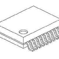
3.5KB Flash, 128B RAM, 18 I/O, CLC, CWG, DDS, 10-bit ADC 20 SSOP .209in TUBE
Manufacturer
Microchip Technology
Series
PIC® 16Fr
Datasheets
1.PIC16F1507-EML.pdf
(266 pages)
2.PIC16F1507-EML.pdf
(26 pages)
3.PIC16F1507-EML.pdf
(40 pages)
Specifications of PIC16F1507-E/SS
Processor Series
PIC16
Core
PIC16F
Data Bus Width
8 bit
Program Memory Type
Flash
Program Memory Size
3.5 KB
Data Ram Size
128 B
Interface Type
ICSP
Maximum Clock Frequency
20 MHz
Number Of Programmable I/os
18
Number Of Timers
3
Operating Supply Voltage
2.3 V to 5.5 V
Maximum Operating Temperature
+ 125 C
Mounting Style
SMD/SMT
Package / Case
SSOP-20
Minimum Operating Temperature
- 40 C
Operating Temperature Range
- 40 C to + 125 C
Supply Current (max)
30 uA
Core Processor
PIC
Core Size
8-Bit
Speed
20MHz
Connectivity
-
Peripherals
Brown-out Detect/Reset, POR, PWM, WDT
Number Of I /o
17
Eeprom Size
-
Ram Size
128 x 8
Voltage - Supply (vcc/vdd)
2.3 V ~ 5.5 V
Data Converters
A/D 12x10b
Oscillator Type
Internal
Operating Temperature
-40°C ~ 125°C
Lead Free Status / Rohs Status
Details


DS41597A-page 12
1.5.1
This is where the device, such as the PIC16F1508, will be selected. When a device is
selected, the program will configure itself automatically to that specific device, such as
data inputs and number of available CLC outputs.
1.5.2
This drop-down menu will display each CLC module. Some devices, such as the
PIC10F320, will only have one available CLC module in the selected device. The “x” in
each CLC register will be replaced by whichever CLC module is used.
1.5.3
There are four input selection groups. Each group consists of 8 selections. For devices
with only 8 inputs, all 8 inputs are available in every group. For devices with 16 inputs,
only 8 of the 16 are available in each group but are distributed in such a way to
minimize precluding some input selection combinations. No input will appear twice in
the same group but will appear as an input in other groups.
As seen in Table 1-2, each drop-down item correlates to a logic cell data input group
(lcxdx). Each data input is selectable at least two different times in two or more different
groups. For example, F
drop-down menus in the CLC tool for a PIC16F1507 as shown in Figure 1-4.
TABLE 1-2:
CLCxIN[0]
CLCxIN[1]
CLCxIN[2]
CLCxIN[3]
CLCxIN[4]
CLCxIN[5]
CLCxIN[6]
CLCxIN[7]
CLCxIN[8]
CLCxIN[9]
CLCxIN[10]
CLCxIN[11]
CLCxIN[12]
CLCxIN[13]
CLCxIN[14]
CLCxIN[15]
Data Input
Device
CLC Module
Data Inputs
CLCX DATA INPUT SELECTION FOR THE PIC16F1507
lcxd1
D1S
000
001
010
011
100
101
110
111
—
—
—
—
—
—
—
—
OSC
could be selected as an input in the first and second
lcxd2
D2S
000
001
010
011
100
101
110
111
—
—
—
—
—
—
—
—
lcxd3
D3S
000
001
010
011
100
101
110
111
—
—
—
—
—
—
—
—
lcxd4
D4S
000
101
110
111
000
001
010
011
—
—
—
—
—
—
—
—
CLC1IN0
CLC1IN1
Reserved
Reserved
F
TMR0IF
TMR1IF
TMR2 = PR2
CLC1OUT
CLC2OUT
Reserved
Reserved
NCO1OUT
HFINTOSC
PWM3OUT
PWM4OUT
OSC
2011 Microchip Technology Inc.
CLC1
CLC2IN0
CLC2IN1
Reserved
Reserved
F
TMR0IF
TMR1IF
TMR2 = PR2
CLC1OUT
CLC2OUT
Reserved
Reserved
ADCFRC
PWM1OUT
PWM2OUT
LFINTOSC
OSC
CLC2
Related parts for PIC16F1507-E/SS
Image
Part Number
Description
Manufacturer
Datasheet
Request
R

Part Number:
Description:
IC, 8BIT MCU, PIC16F, 32MHZ, SOIC-18
Manufacturer:
Microchip Technology
Datasheet:

Part Number:
Description:
IC, 8BIT MCU, PIC16F, 32MHZ, SSOP-20
Manufacturer:
Microchip Technology
Datasheet:

Part Number:
Description:
IC, 8BIT MCU, PIC16F, 32MHZ, DIP-18
Manufacturer:
Microchip Technology
Datasheet:

Part Number:
Description:
IC, 8BIT MCU, PIC16F, 32MHZ, QFN-28
Manufacturer:
Microchip Technology
Datasheet:

Part Number:
Description:
IC, 8BIT MCU, PIC16F, 32MHZ, QFN-28
Manufacturer:
Microchip Technology
Datasheet:
Part Number:
Description:
IC, 8BIT MCU, PIC16F, 32MHZ, QFN-28
Manufacturer:
Microchip Technology
Datasheet:
Part Number:
Description:
IC, 8BIT MCU, PIC16F, 32MHZ, SSOP-20
Manufacturer:
Microchip Technology
Datasheet:

Part Number:
Description:
IC, 8BIT MCU, PIC16F, 20MHZ, DIP-40
Manufacturer:
Microchip Technology
Datasheet:

Part Number:
Description:
IC, 8BIT MCU, PIC16F, 32MHZ, QFN-28
Manufacturer:
Microchip Technology
Datasheet:

Part Number:
Description:
IC, 8BIT MCU, PIC16F, 20MHZ, MQFP-44
Manufacturer:
Microchip Technology
Datasheet:

Part Number:
Description:
IC, 8BIT MCU, PIC16F, 20MHZ, QFN-20
Manufacturer:
Microchip Technology
Datasheet:
Part Number:
Description:
IC, 8BIT MCU, PIC16F, 32MHZ, QFN-28
Manufacturer:
Microchip Technology
Datasheet:

Part Number:
Description:
MCU 14KB FLASH 768B RAM 64-TQFP
Manufacturer:
Microchip Technology
Datasheet:
Part Number:
Description:
7 KB Flash, 384 Bytes RAM, 32 MHz Int. Osc, 16 I/0, Enhanced Mid Range Core, Low
Manufacturer:
Microchip Technology

Part Number:
Description:
14KB Flash, 512B RAM, 256B EEPROM, LCD, 1.8-5.5V 40 UQFN 5x5x0.5mm TUBE
Manufacturer:
Microchip Technology
Datasheet: