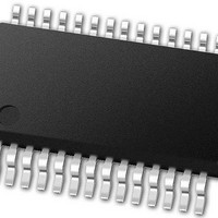
PIC24FJ64GA102-E/SS Microchip Technology, PIC24FJ64GA102-E/SS Datasheet - Page 260

PIC24FJ64GA102-E/SS
Manufacturer Part Number
PIC24FJ64GA102-E/SS
Description
16-bit, 16 MIPS, 64KB Flash, 8KB RAM, Nanowatt XLP 28 SSOP .209in TUBE
Manufacturer
Microchip Technology
Series
PIC® XLP™ 24Fr
Datasheet
1.PIC24FJ32GA102-ISP.pdf
(308 pages)
Specifications of PIC24FJ64GA102-E/SS
Processor Series
PIC24
Core
PIC24F
Data Bus Width
16 bit
Program Memory Type
Flash
Program Memory Size
64 KB
Data Ram Size
8192 B
Interface Type
I2C, SPI, UART
Maximum Clock Frequency
32 MHz
Number Of Programmable I/os
21
Number Of Timers
5
Operating Supply Voltage
2 V to 3.6 V
Maximum Operating Temperature
+ 125 C
Mounting Style
SMD/SMT
Package / Case
SSOP-28
Development Tools By Supplier
MPLAB Integrated Development Environment
Minimum Operating Temperature
- 40 C
Operating Temperature Range
- 40 C to + 125 C
Supply Current (max)
300 mA
Core Processor
PIC
Core Size
16-Bit
Speed
32MHz
Connectivity
I²C, IrDA, SPI, UART/USART
Peripherals
Brown-out Detect/Reset, LVD, POR, PWM, WDT
Number Of I /o
21
Eeprom Size
-
Ram Size
8K x 8
Voltage - Supply (vcc/vdd)
2 V ~ 3.6 V
Data Converters
A/D 10x10b
Oscillator Type
Internal
Operating Temperature
-40°C ~ 125°C
Lead Free Status / Rohs Status
Details
- Current page: 260 of 308
- Download datasheet (3Mb)
PIC24FJ64GA104 FAMILY
TABLE 27-2:
DS39951C-page 260
PWRSAV
RCALL
REPEAT
RESET
RETFIE
RETLW
RETURN
RLC
RLNC
RRC
RRNC
SE
SETM
SL
SUB
SUBB
SUBR
SUBBR
SWAP
Mnemonic
Assembly
PWRSAV
RCALL
RCALL
REPEAT
REPEAT
RESET
RETFIE
RETLW
RETURN
RLC
RLC
RLC
RLNC
RLNC
RLNC
RRC
RRC
RRC
RRNC
RRNC
RRNC
SE
SETM
SETM
SETM
SL
SL
SL
SL
SL
SUB
SUB
SUB
SUB
SUB
SUBB
SUBB
SUBB
SUBB
SUBB
SUBR
SUBR
SUBR
SUBR
SUBBR
SUBBR
SUBBR
SUBBR
SWAP.b
SWAP
INSTRUCTION SET OVERVIEW (CONTINUED)
#lit1
Expr
Wn
#lit14
Wn
#lit10,Wn
f
f,WREG
Ws,Wd
f
f,WREG
Ws,Wd
f
f,WREG
Ws,Wd
f
f,WREG
Ws,Wd
Ws,Wnd
f
WREG
Ws
f
f,WREG
Ws,Wd
Wb,Wns,Wnd
Wb,#lit5,Wnd
f
f,WREG
#lit10,Wn
Wb,Ws,Wd
Wb,#lit5,Wd
f
f,WREG
#lit10,Wn
Wb,Ws,Wd
Wb,#lit5,Wd
f
f,WREG
Wb,Ws,Wd
Wb,#lit5,Wd
f
f,WREG
Wb,Ws,Wd
Wb,#lit5,Wd
Wn
Wn
Assembly Syntax
Go into Sleep or Idle mode
Relative Call
Computed Call
Repeat Next Instruction lit14 + 1 times
Repeat Next Instruction (Wn) + 1 times
Software Device Reset
Return from Interrupt
Return with Literal in Wn
Return from Subroutine
f = Rotate Left through Carry f
WREG = Rotate Left through Carry f
Wd = Rotate Left through Carry Ws
f = Rotate Left (No Carry) f
WREG = Rotate Left (No Carry) f
Wd = Rotate Left (No Carry) Ws
f = Rotate Right through Carry f
WREG = Rotate Right through Carry f
Wd = Rotate Right through Carry Ws
f = Rotate Right (No Carry) f
WREG = Rotate Right (No Carry) f
Wd = Rotate Right (No Carry) Ws
Wnd = Sign-Extended Ws
f = FFFFh
WREG = FFFFh
Ws = FFFFh
f = Left Shift f
WREG = Left Shift f
Wd = Left Shift Ws
Wnd = Left Shift Wb by Wns
Wnd = Left Shift Wb by lit5
f = f – WREG
WREG = f – WREG
Wn = Wn – lit10
Wd = Wb – Ws
Wd = Wb – lit5
f = f – WREG – (C)
WREG = f – WREG – (C)
Wn = Wn – lit10 – (C)
Wd = Wb – Ws – (C)
Wd = Wb – lit5 – (C)
f = WREG – f
WREG = WREG – f
Wd = Ws – Wb
Wd = lit5 – Wb
f = WREG – f – (C)
WREG = WREG – f – (C)
Wd = Ws – Wb – (C)
Wd = lit5 – Wb – (C)
Wn = Nibble Swap Wn
Wn = Byte Swap Wn
Description
2010 Microchip Technology Inc.
Words
# of
1
1
1
1
1
1
1
1
1
1
1
1
1
1
1
1
1
1
1
1
1
1
1
1
1
1
1
1
1
1
1
1
1
1
1
1
1
1
1
1
1
1
1
1
1
1
1
1
1
1
Cycles
3 (2)
3 (2)
3 (2)
# of
1
2
2
1
1
1
1
1
1
1
1
1
1
1
1
1
1
1
1
1
1
1
1
1
1
1
1
1
1
1
1
1
1
1
1
1
1
1
1
1
1
1
1
1
1
1
1
WDTO, Sleep
None
None
None
None
None
None
None
None
C, N, Z
C, N, Z
C, N, Z
N, Z
N, Z
N, Z
C, N, Z
C, N, Z
C, N, Z
N, Z
N, Z
N, Z
C, N, Z
None
None
None
C, N, OV, Z
C, N, OV, Z
C, N, OV, Z
N, Z
N, Z
C, DC, N, OV, Z
C, DC, N, OV, Z
C, DC, N, OV, Z
C, DC, N, OV, Z
C, DC, N, OV, Z
C, DC, N, OV, Z
C, DC, N, OV, Z
C, DC, N, OV, Z
C, DC, N, OV, Z
C, DC, N, OV, Z
C, DC, N, OV, Z
C, DC, N, OV, Z
C, DC, N, OV, Z
C, DC, N, OV, Z
C, DC, N, OV, Z
C, DC, N, OV, Z
C, DC, N, OV, Z
C, DC, N, OV, Z
None
None
Status Flags
Affected
Related parts for PIC24FJ64GA102-E/SS
Image
Part Number
Description
Manufacturer
Datasheet
Request
R

Part Number:
Description:
Manufacturer:
Microchip Technology Inc.
Datasheet:

Part Number:
Description:
Manufacturer:
Microchip Technology Inc.
Datasheet:

Part Number:
Description:
Manufacturer:
Microchip Technology Inc.
Datasheet:

Part Number:
Description:
Manufacturer:
Microchip Technology Inc.
Datasheet:

Part Number:
Description:
Manufacturer:
Microchip Technology Inc.
Datasheet:

Part Number:
Description:
Manufacturer:
Microchip Technology Inc.
Datasheet:

Part Number:
Description:
Manufacturer:
Microchip Technology Inc.
Datasheet:

Part Number:
Description:
Manufacturer:
Microchip Technology Inc.
Datasheet:


