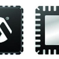
PIC24FV32KA302-E/ML Microchip Technology, PIC24FV32KA302-E/ML Datasheet - Page 131

PIC24FV32KA302-E/ML
Manufacturer Part Number
PIC24FV32KA302-E/ML
Description
32KB Flash, 2KB RAM, 512B EEPROM, 16 MIPS, 12-bit ADC, CTMU, 5V 28 QFN 6x6mm TUB
Manufacturer
Microchip Technology
Series
PIC® XLP™ 24Fr
Datasheet
1.PIC24F16KA301T-ISO.pdf
(320 pages)
Specifications of PIC24FV32KA302-E/ML
Processor Series
PIC24FV
Core
PIC
Data Bus Width
16 bit
Program Memory Type
Flash
Program Memory Size
32 KB
Data Ram Size
2 KB
Maximum Operating Temperature
+ 125 C
Mounting Style
SMD/SMT
Package / Case
QFN-28
Development Tools By Supplier
MPLAB IDE Software
Minimum Operating Temperature
- 40 C
Core Processor
PIC
Core Size
16-Bit
Speed
32MHz
Connectivity
I²C, IrDA, LIN, SPI, UART/USART
Peripherals
Brown-out Detect/Reset, HLVD, POR, PWM, WDT
Number Of I /o
23
Eeprom Size
512 x 8
Ram Size
2K x 8
Voltage - Supply (vcc/vdd)
2 V ~ 5.5 V
Data Converters
A/D 13x12b
Oscillator Type
Internal
Operating Temperature
-40°C ~ 125°C
Lead Free Status / Rohs Status
Details
- Current page: 131 of 320
- Download datasheet (3Mb)
REGISTER 10-1:
2011 Microchip Technology Inc.
bit 15
bit 7
Legend:
R = Readable bit
-n = Value at POR
bit 15
bit 14-9
bit 8
bit 7-3
bit 2
bit 1
bit 0
Note 1:
R/W-0
DSEN
U-0
—
2:
All register bits are reset only in the case of a POR event outside of Deep Sleep mode.
Unlike all other events, a Deep Sleep BOR event will NOT cause a wake-up from Deep Sleep; this re-arms
POR.
DSEN: Deep Sleep Enable bit
1 = Enters Deep Sleep on execution of PWRSAV #0
0 = Enters normal Sleep on execution of PWRSAV #0
Unimplemented: Read as ‘0’
RTCCWDIS: RTCC Wake-up Disable bit
1 = Wake-up from Deep Sleep with RTCC disabled
0 = Wake-up from Deep Sleep with RTCC enabled
Unimplemented: Read as ‘0’
ULPWUDIS: ULPWU Wake-up Disable bit
1 = Wake-up from Deep Sleep with ULPWU disabled
0 = Wake-up from Deep Sleep with ULPWU enabled
DSBOR: Deep Sleep BOR Event bit
1 = The DSBOR was active and a BOR event was detected during Deep Sleep
0 = The DSBOR was not active, or was active but did not detect a BOR event during Deep Sleep
RELEASE: I/O Pin State Release bit
1 = Upon waking from Deep Sleep, I/O pins maintain their previous states to Deep Sleep entry
0 = Release I/O pins from their state previous to Deep Sleep entry, and allow their respective TRIS and
LAT bits to control their states
U-0
U-0
—
—
DSCON: DEEP SLEEP CONTROL REGISTER
C = Clearable bit
W = Writable bit
‘1’ = Bit is set
U-0
U-0
—
—
U-0
U-0
PIC24FV32KA304 FAMILY
—
—
(2)
HS = Hardware Settable bit
U = Unimplemented bit, read as ‘0’
‘0’ = Bit is cleared
U-0
U-0
—
—
ULPWUDIS
(1)
R/W-0
U-0
—
x = Bit is unknown
DSBOR
R/W-0
U-0
—
(2)
DS39995B-page 131
RTCCWDIS
R/C-0, HS
RELEASE
R/W-0
bit 8
bit 0
Related parts for PIC24FV32KA302-E/ML
Image
Part Number
Description
Manufacturer
Datasheet
Request
R

Part Number:
Description:
Manufacturer:
Microchip Technology Inc.
Datasheet:

Part Number:
Description:
Manufacturer:
Microchip Technology Inc.
Datasheet:

Part Number:
Description:
Manufacturer:
Microchip Technology Inc.
Datasheet:

Part Number:
Description:
Manufacturer:
Microchip Technology Inc.
Datasheet:

Part Number:
Description:
Manufacturer:
Microchip Technology Inc.
Datasheet:

Part Number:
Description:
Manufacturer:
Microchip Technology Inc.
Datasheet:

Part Number:
Description:
Manufacturer:
Microchip Technology Inc.
Datasheet:

Part Number:
Description:
Manufacturer:
Microchip Technology Inc.
Datasheet:


