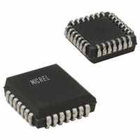
SY89430VJZ Micrel Inc, SY89430VJZ Datasheet - Page 4

SY89430VJZ
Manufacturer Part Number
SY89430VJZ
Description
5V/3.3V Programmable Frequency Synthesizer (50-950MHz) ( )
Manufacturer
Micrel Inc
Series
Precision Edge®r
Type
Frequency Synthesizerr
Datasheet
1.SY89430VZH.pdf
(11 pages)
Specifications of SY89430VJZ
Pll
Yes
Input
Crystal
Output
PECL
Number Of Circuits
1
Ratio - Input:output
1:1
Differential - Input:output
No/Yes
Frequency - Max
950MHz
Divider/multiplier
Yes/No
Voltage - Supply
3.135 V ~ 5.25 V
Operating Temperature
0°C ~ 75°C
Mounting Type
Surface Mount
Package / Case
28-LCC (J-Lead)
Frequency-max
950MHz
Number Of Elements
1
Supply Current
220mA
Pll Input Freq (min)
10MHz
Pll Input Freq (max)
25MHz
Operating Supply Voltage (typ)
3.3/5V
Operating Temp Range
0C to 75C
Package Type
PLCC
Output Frequency Range
50 to 950MHz
Operating Supply Voltage (min)
3.135V
Operating Supply Voltage (max)
5.25V
Operating Temperature Classification
Commercial
Pin Count
28
Lead Free Status / RoHS Status
Lead free / RoHS Compliant
Other names
576-2560
SY89430VJZ
SY89430VJZ
Available stocks
Company
Part Number
Manufacturer
Quantity
Price
Company:
Part Number:
SY89430VJZ
Manufacturer:
Microchip
Quantity:
1 905
Micrel, Inc.
INPUTS
XTAL1, XTAL2
These pins form an oscillator when connected to an external
crystal. The crystal is series resonant. See “AN-07” for
Crystal Interface Guideline.
S_
This TTL pin loads the configuration latches with the contents
of the shift registers. The latches will be transparent when this
signal is HIGH; thus, the register data must be stable on the
HIGH-to-LOW transition of S_
S_
This TTL pin is the input to the serial configuration shift
registers.
S_
This TTL pin clocks the serial configuration shift registers. On
the rising edge of this signal, data from S_
/P_
This TTL pin loads the configuration latches with the contents
of the parallel inputs. The latches will be transparent when this
signal is LOW; thus, the parallel data must be stable on the
LOW-to-HIGH transition of /P_
M[8:0]
These TTL pins are used to configure the PLL loop divider.
They are sampled on the LOW-to-HIGH transition of /P_
M[8] is the MSB, M[0] is the LSB. The binary count on the M
pins equates to the divide-by value for the PLL.
N[1:0]
These TTL pins are used to configure the output divider
modulus. They are sampled on the LOW-to-HIGH transition
of /P_
M9999-011106
hbwhelp@micrel.com or (408) 955-1690
PIN DESCRIPTIONS
LOAD
DATA
CLOCK
LOAD
LOAD
N[1:0]
0 0
0 1
1 0
1 1
.
LOAD
LOAD
Output Division
for proper operation.
for proper operation.
2
4
8
1
DATA
is sampled.
LOAD
.
4
OUTPUTS
FOUT, FOUT
These differential positive-referenced ECL signals (PECL)
are the output of the synthesizer.
TEST
The function of this TTL output is determined by the serial
configuration bits T[2:0].
POWER
V
This is the positive supply for the chip and is normally
connected to +3.3V or +5.0V.
V
This is the positive reference for the PECL outputs, FOUT and
/FOUT. It is constrained to be less than or equal to
V
This is the positive supply for the PLL and should be as noise-
free as possible for low-jitter operation.
GND
These pins are the negative supply for the chip and are
normally all connected to ground.
OTHER
LOOP_FILTER
This is an analog I/O pin that provides the loop filter for the
PLL.
LOOP_REF
This is an analog I/O pin that provides a reference voltage for
the PLL.
CC1
CC_OUT
CC_QUIET
Precision Edge
SY89430V
VCC1
.
®


