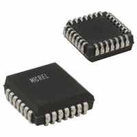
SY89430VJZ Micrel Inc, SY89430VJZ Datasheet - Page 5

SY89430VJZ
Manufacturer Part Number
SY89430VJZ
Description
5V/3.3V Programmable Frequency Synthesizer (50-950MHz) ( )
Manufacturer
Micrel Inc
Series
Precision Edge®r
Type
Frequency Synthesizerr
Datasheet
1.SY89430VZH.pdf
(11 pages)
Specifications of SY89430VJZ
Pll
Yes
Input
Crystal
Output
PECL
Number Of Circuits
1
Ratio - Input:output
1:1
Differential - Input:output
No/Yes
Frequency - Max
950MHz
Divider/multiplier
Yes/No
Voltage - Supply
3.135 V ~ 5.25 V
Operating Temperature
0°C ~ 75°C
Mounting Type
Surface Mount
Package / Case
28-LCC (J-Lead)
Frequency-max
950MHz
Number Of Elements
1
Supply Current
220mA
Pll Input Freq (min)
10MHz
Pll Input Freq (max)
25MHz
Operating Supply Voltage (typ)
3.3/5V
Operating Temp Range
0C to 75C
Package Type
PLCC
Output Frequency Range
50 to 950MHz
Operating Supply Voltage (min)
3.135V
Operating Supply Voltage (max)
5.25V
Operating Temperature Classification
Commercial
Pin Count
28
Lead Free Status / RoHS Status
Lead free / RoHS Compliant
Other names
576-2560
SY89430VJZ
SY89430VJZ
Available stocks
Company
Part Number
Manufacturer
Quantity
Price
Company:
Part Number:
SY89430VJZ
Manufacturer:
Microchip
Quantity:
1 905
the basis of its frequency reference. The output of the reference
oscillator is divided by eight before being sent to the phase
detector. With a 16MHz crystal, this provides a reference
frequency of 2MHz.
950MHz. Its output is scaled by a divider that is configured by
either the serial or parallel interfaces. The output of this loop
divider is also applied to the phase detector.
frequency to be M times the reference frequency by adjusting
the VCO control voltage. Note that for some values of M
(either too high or too low) the PLL will not achieve loop lock.
External loop filter components are utilized to allow for optimal
phase jitter performance.
divider before being sent to the PECL output driver. The
output divider is configured through either the serial or the
parallel interfaces and can provide one of four divider ratios
(1, 2, 4 or 8). This divider extends the performance of the part
while providing a 50% duty cycle.
divider and is capable of driving a pair of transmission lines
terminated in 50Ω to V
the output driver is provided by a dedicated power pin
(V
Micrel, Inc.
M9999-011106
hbwhelp@micrel.com or (408) 955-1690
FUNCTIONAL DESCRIPTION
WITH 16MHZ INPUT
CC_OUT
The internal oscillator uses the external quartz crystal as
The VCO within the PLL operates over a range of 400–
The phase detector and loop filter force the VCO output
The output of the VCO is also passed through an output
The output driver is driven differentially from the output
VCO Frequency
(MHz)
400
402
404
406
944
946
948
950
) to reduce noise induced jitter.
•
•
•
CC
–2volts. The positive reference for
M Count
200
201
202
203
472
473
474
475
•
•
•
256
M8
0
0
0
0
1
1
1
1
•
•
•
128
M7
1
1
1
1
1
1
1
1
•
•
•
M6
64
1
1
1
1
1
1
1
1
•
•
•
5
parallel. The parallel interface uses the values at the M[8:0]
and N[1:0] inputs to configure the internal counters.
Normally, upon system reset, the P_
LOW until some time after power becomes valid. With
S_
P_
interface has priority over the serial interface. Internal pull-
up resistors are provided on the M[8:0] and N[1:0] inputs to
reduce component count.
register scheme. The register shifts once per rising edge of the
S_
hold timing as specified in the AC parameters section of this
data sheet. With P_
will capture the value in the shift register on the HIGH-to-LOW
edge of the S_
more information.
is controlled by the T[2:0] bits in the serial data stream. See
the programming subsection of this data sheet for more
information.
The configuration logic has two sections: serial and
The serial interface logic is implemented with a 14-bit shift
The TEST output reflects various internal node values and
CLOCK
LOAD
LOAD
M5
32
0
0
0
0
0
0
0
0
•
•
•
, the parallel inputs are captured. The parallel
held LOW, on the LOW-to-HIGH transition of
input. The serial input S_
LOAD
M4
16
0
0
0
0
1
1
1
1
•
•
•
LOAD
input. See the programming section for
held HIGH, the configuration latches
M3
8
1
1
1
1
1
1
1
1
•
•
•
DATA
M2
4
0
0
0
0
0
0
0
0
•
•
•
must meet set-up and
LOAD
Precision Edge
M1
2
0
0
1
1
0
0
1
1
•
•
•
input is held
SY89430V
M0
1
0
1
0
1
0
1
0
1
•
•
•
®


