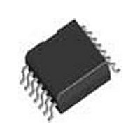
MF6CWM-100 National Semiconductor, MF6CWM-100 Datasheet - Page 5

MF6CWM-100
Manufacturer Part Number
MF6CWM-100
Description
Manufacturer
National Semiconductor
Datasheet
1.MF6CWM-100.pdf
(20 pages)
Specifications of MF6CWM-100
Architecture
Switched Capacitor
Dual Supply Voltage (typ)
±3/±5V
Power Supply Requirement
Single/Dual
Single Supply Voltage (min)
5V
Dual Supply Voltage (min)
±2.5V
Operating Temperature (min)
0C
Operating Temperature (max)
70C
Operating Temperature Classification
Commercial
Package Type
SOIC W
Filter Type
Low Pass Filter
Lead Free Status / RoHS Status
Not Compliant
Available stocks
Company
Part Number
Manufacturer
Quantity
Price
Company:
Part Number:
MF6CWM-100
Manufacturer:
NS
Quantity:
5 510
Company:
Part Number:
MF6CWM-100
Manufacturer:
QTC
Quantity:
5 510
Part Number:
MF6CWM-100
Manufacturer:
NS/国半
Quantity:
20 000
Logic Input-Output Electrical Characteristics
Note 4: Besides checking the cutoff frequency (f
filter. The magnitudes are referenced to a DC gain of 0.0 dB.
Note 5: For simplicity all the logic levels have been referenced to V
els).
Note 6: The short circuit source current is measured by forcing the output that is being tested to its maximum positive voltage swing and then shorting that output
to the negative supply. The short circuit sink current is measured by forcing the output that is being tested to its maximum negative voltage swing and then shorting
that output to the positive supply. These are the worst-case conditions.
Note 7: The MF6 is operating with symmetrical split supplies and L.Sh is tied to ground.
Note 8: Typicals are at 25˚C and represent most likely parametric norm.
Note 9: Tested limits are guaranteed to National’s AOQL (Average Outgoing Quality Level).
Note 10: Design limits are guaranteed, but not 100% tested. These limits are not used to calculate outgoing quality levels.
Note 11: Absolute Maximum Ratings indicate limits beyond which damage to the device may occur. DC and AC electrical specifications do not apply when operating
the device beyond its specified conditions.
Note 12: Human body model, 100 pF discharged through a 1.5k
Note 13: When the input voltage (V
to 5 mA or less. The 20 mA package input current limits the number of pins that can exceed the power supply boundaries with a 5 mA current limit to four.
Note 14: The maximum power dissipation must be derated at elevated temperatures and is dictated by T
allowable power dissipation at any temperature is P
T
Typical Performance Characteristics
Schmitt Trigger Threshold Voltage
vs Power Supply Voltage
Crosstalk from Filter
to Op-Amps (MF6-50)
JMAX
= 125˚C, and the typical junction-to-ambient thermal resistance is 78˚C/W. For the MF6CJ this number decreases to 62˚C/W. For MF6CWM,
DS005065-40
IN
DS005065-43
) at any pin exceeds the power supply rails (V
c
) and the stopband attenuation at 2 f
D
= (T
Crosstalk from Filter
to Op-Amps (MF6-100)
Crosstalk from Either Op-Amp to
Filter Output (MF6-100)
JMAX
− T
A
−
)/
resistor.
= 0V and will scale accordingly for
JA
or the number given in the Absolute Maximum Ratings, whichever is lower. For this device,
5
IN
c
, two additional frequencies are used to check the magnitude response of the
<
V
−
or V
DS005065-41
DS005065-44
IN
(Continued)
>
V
+
±
) the absolute value of current at that pin should be limited
JMAX
5V and
,
JA
±
Crosstalk from Either Op-Amp
to Filter Output (MF6-50)
Equivalent Input Noise
Voltage of Op-Amps
, and the ambient temperature, T
2.5V supplies (except for the TTL input logic lev-
A
. The maximum
www.national.com
DS005065-45
DS005065-42
JA
= 78˚C/W.


