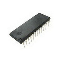
LM1207N National Semiconductor, LM1207N Datasheet

LM1207N
Specifications of LM1207N
Available stocks
Related parts for LM1207N
LM1207N Summary of contents
Page 1
... High resolution RGB CRT monitors Y Video AGC amplifiers Y Wideband amplifiers with gain and DC offset controls Y Interface amplifiers for LCD or CCD systems Y FIGURE 1 Order Number LM1205N or LM1207N See NS Package Number N28B RRD-B30M66 Printed January 1996 range output swing (slight reduction 11881 – 1 ...
Page 2
... Absolute Maximum Ratings If Military Aerospace specified devices are required please contact the National Semiconductor Sales Office Distributors for availability and specifications Supply Voltage ( Pins (Note 3) Peak Video Output Source Current (Any One Amp) Pins Voltage at Any Input Pin ( Power Dissipation ( (Above 25 C Derate Based on ...
Page 3
AC Electrical Characteristics adjust Video Output pins 17 20 and for the AC test unless otherwise stated (Note 14) Symbol Parameter A Video Amplifier Gain V max A Attenuation Attenuation 0 25V ...
Page 4
Typical Performance Characteristics Attenuation vs Contrast Voltage LM1205 Crosstalk vs Frequency LM1205 Contrast vs Frequency LM1205 Drive vs Frequency http www national com V 12V unless otherwise specified Attenuation vs Drive Voltage TL ...
Page 5
Typical Performance Characteristics LM1207 Crosstalk vs Frequency LM1207 Contrast vs Frequency LM1207 Drive vs Frequency V 12V unless otherwise specified (Continued 11881 – 11881 – ...
Page 6
... Applications Information FIGURE 2 LM1205N LM1207N DC Test Circuit http www national com 11881 – 10 ...
Page 7
... Applications Information (Continued) FIGURE 3 LM1205N LM1207N AC Test Circuit 11881– 11 http www national com ...
Page 8
... Applications Information FIGURE 4 LM1205N LM1207N PCB Test Circuit http www national com (Continued 11881 – 12 ...
Page 9
Applications Information (Continued) Figure 5 shows the block diagram of a typical analog RGB color monitor The RGB monitor is used with CAD CAM work stations PC’s arcade games and in a wide range of other applications that benefit from ...
Page 10
Functional Description (Continued) The drive control signal comes in on pin 18 Each channel has its own drive section therefore the crosstalk compensation needed for the contrast control voltages is not required for the drive control thus ...
Page 11
Functional Description (Continued) FIGURE 6 Block Diagram of LM1205 LM1207 Video Amplifier FIGURE 7 Timing Diagram Circuit Description VIDEO AMPLIFIER INPUT STAGE Figure simplified schematic of one of the three video amplifiers input stage along with the ...
Page 12
Circuit Description (Continued) and R4 is used to compensate for beta variations of the transistors Note that the bias voltage passes through three diode drops (Q5 Q6 and Q7) before setting the voltage across and Q4 also ...
Page 13
Circuit Description (Continued) CONTRAST CONTROL Figure simplified schematic of the Contrast Control circuit The output of this circuit is common to all three chan- nels A reference voltage is generated by Z2 Q34 Q35 R30 and R31 ...
Page 14
Circuit Description (Continued) FIGURE 9 Simplified Schematic of LM1205 LM1207 Contrast Control FIGURE 10 Simplified Schematic of LM1205 LM1207 Drive Control http www national com 11881 – 11881 – 18 ...
Page 15
Circuit Description (Continued) CLAMP COMPARATOR CIRCUIT Figure simplified schematic of the clamp comparator circuit Q85 and its input transistors Q81 and Q82 are one half of the differential pair The base of Q81 is connected to pin ...
Page 16
Circuit Description (Continued) FIGURE 11 Simplified Schematic of LM1205 LM1207 Clamp Comparator Circuit CLAMP GATE CIRCUIT Figure simplified schematic of the Clamp Gate cir- cuit A voltage reference is setup by Z3 and by Q104 and Q105 ...
Page 17
Circuit Description (Continued) comparators of the three video channels Q103 is added to help drive the base of Q86 in the clamp comparator in- creasing the accuracy of the current mirror Q101 drives R79 and R80 This sets the current ...
Page 18
Circuit Description (Continued) FIGURE 13 Simplified Schematic of LM1205 LM1207 Blank Gate Circuit VIDEO AMPLIFIER OUTPUT STAGE WITH BLANK CIRCUIT Figure simplified schematic of the Video Amplifier Output Stage including the blanking circuit Q18 serves as a ...
Page 19
Circuit Description (Continued) age of Q29 There are also four diode drops from the base of Q30 to the output pin 20 Therefore during blanking pin 20 will be less than 100 mV above ground enabling the designer to blank ...
Page 20
... LM1205 LM1207 is designed into a video board one must keep the ground to the CRT driver stage separate from the ground of the LM1205 LM1207 grounds together only at one point National Semiconductor also manufactures a line of CRT drivers Please contact Na- tional for additional information These drivers greatly simpli- ...
Page 21
Applications of the LM1205 LM1207 FIGURE 16 Demonstration Board Layout (Continued 11881– 24 http www national com ...
Page 22
Applications of the LM1205 LM1207 FIGURE 17a LM1205 Rise Time FIGURE 17c LM1207 Rise Time FIGURE 18 LM1205 LM1207 Typical Application http www national com (Continued 11881– 25 FIGURE 17b LM1205 Fall Time TL H 11881– 27 FIGURE ...
Page 23
23 http www national com ...
Page 24
... Physical Dimensions inches (millimeters) unless otherwise noted Order Number LM1205N or LM1207N LIFE SUPPORT POLICY NATIONAL’S PRODUCTS ARE NOT AUTHORIZED FOR USE AS CRITICAL COMPONENTS IN LIFE SUPPORT DEVICES OR SYSTEMS WITHOUT THE EXPRESS WRITTEN APPROVAL OF THE PRESIDENT OF NATIONAL SEMICONDUCTOR CORPORATION As used herein 1 Life support devices or systems are devices or ...


