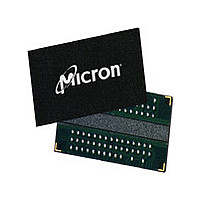
MT47H32M16HR-25E IT:F Micron Technology Inc, MT47H32M16HR-25E IT:F Datasheet - Page 28

MT47H32M16HR-25E IT:F
Manufacturer Part Number
MT47H32M16HR-25E IT:F
Description
Manufacturer
Micron Technology Inc
Type
DDR2 SDRAMr
Datasheet
1.MT47H32M16HR-25E_ITF.pdf
(132 pages)
Specifications of MT47H32M16HR-25E IT:F
Organization
32Mx16
Density
512Mb
Address Bus
15b
Access Time (max)
400ps
Maximum Clock Rate
800MHz
Operating Supply Voltage (typ)
1.8V
Package Type
FBGA
Operating Temp Range
-40C to 85C
Operating Supply Voltage (max)
1.9V
Operating Supply Voltage (min)
1.7V
Supply Current
295mA
Pin Count
84
Mounting
Surface Mount
Operating Temperature Classification
Industrial
Lead Free Status / RoHS Status
Compliant
- Current page: 28 of 132
- Download datasheet (10Mb)
Table 11: DDR2 I
Notes: 1–7 apply to the entire table
PDF: 09005aef82f1e6e2
512MbDDR2.pdf - Rev. R 12/10 EN
Parameter/Condition
Operating one bank active-pre-
charge current:
t
HIGH, CS# is HIGH between valid com-
mands; address bus inputs are switch-
ing; Data bus inputs are switching
Operating one bank active-read-
precharge current: I
4, CL = CL (I
t
t
HIGH between valid commands; ad-
dress bus inputs are switching; Data
pattern is same as I
Precharge power-down current:
All banks idle;
LOW; Other control and address bus
inputs are stable; Data bus inputs are
floating
Precharge quiet standby current:
All banks idle;
HIGH, CS# is HIGH; Other control and
address bus inputs are stable; Data
bus inputs are floating
Precharge standby current: All
banks idle;
HIGH, CS# is HIGH; Other control and
address bus inputs are switching; Da-
ta bus inputs are switching
Active power-down current: All
banks open;
LOW; Other control and address bus
inputs are stable; Data bus inputs are
floating
Active standby current: All banks
open;
MAX (I
HIGH, CS# is HIGH between valid com-
mands; Other control and address bus
inputs are switching; Data bus inputs
are switching
RC (I
RC =
RCD =
DD
t
RC (I
t
DD
CK =
t
),
RCD (I
),
t
RAS =
DD
t
t
DD
RP =
CK =
t
t
CK (I
),
CK =
), AL = 0;
DD
t
t
t
CK =
CK =
RAS =
); CKE is HIGH, CS# is
t
t
RAS MIN (I
t
t
DD
RP (I
CK (I
CK =
t
DD4W
CK (I
DD
),
t
t
CK (I
CK (I
t
DD
OUT
t
RAS =
DD
RAS MIN (I
Specifications and Conditions (Die Revision G)
t
t
CK (I
CK =
DD
); CKE is
); CKE is
= 0mA; BL =
DD
DD
); CKE is
DD
); CKE is
); CKE is
DD
t
t
RAS
CK (I
); CKE is
),
t
DD
RC =
DD
),
),
Symbol
I
I
I
I
I
I
DD3Pf
DD3Ps
I
I
DD2Q
DD2N
DD3N
DD2P
DD0
DD1
Slow PDN exit
Fast PDN exit
Configura-
x4, x8, x16
MR12 = 0
MR12 = 1
x4, x8
x4, x8
x4, x8
x4, x8
x4, x8
tion
x16
x16
x16
x16
x16
28
Electrical Specifications – I
-187E
TBD
TBD
TBD
TBD
TBD
TBD
TBD
TBD
TBD
TBD
TBD
TBD
TBD
Micron Technology, Inc. reserves the right to change products or specifications without notice.
512Mb: x4, x8, x16 DDR2 SDRAM
-25E/
-25
65
80
75
95
24
26
28
30
18
33
35
7
9
-3E/-3
60
75
70
90
22
24
25
27
15
30
32
7
9
-37E
© 2004 Micron Technology, Inc. All rights reserved.
55
70
65
85
20
22
23
25
14
27
29
7
9
DD
-5E
55
70
65
85
19
20
21
23
13
24
26
7
9
Parameters
Units
mA
mA
mA
mA
mA
mA
mA
Related parts for MT47H32M16HR-25E IT:F
Image
Part Number
Description
Manufacturer
Datasheet
Request
R

Part Number:
Description:
IC DDR2 SDRAM 512MBIT 84FBGA
Manufacturer:
Micron Technology Inc
Datasheet:

Part Number:
Description:
IC DDR2 SDRAM 512MBIT 3NS 84FBGA
Manufacturer:
Micron Technology Inc
Datasheet:

Part Number:
Description:
32MX16 DDR2 SDRAM PLASTIC IND TEMP PBF FBGA 1.8V
Manufacturer:
Micron Technology Inc
Datasheet:

Part Number:
Description:
DRAM Chip DDR2 SDRAM 512M-Bit 32Mx16 1.8V 84-Pin FBGA T/R
Manufacturer:
Micron Technology Inc
Datasheet:

Part Number:
Description:
Manufacturer:
Micron Technology Inc
Datasheet:

Part Number:
Description:
Manufacturer:
Micron Technology Inc
Datasheet:

Part Number:
Description:
Manufacturer:
Micron Technology Inc
Datasheet:

Part Number:
Description:
MICMT47H32M16HR-3_IT:F 32MBX16 DDR2
Manufacturer:
Micron Technology Inc
Datasheet:

Part Number:
Description:
Manufacturer:
Micron Technology Inc
Datasheet:

Part Number:
Description:
Manufacturer:
Micron Technology Inc
Datasheet:

Part Number:
Description:
Manufacturer:
Micron Technology Inc
Datasheet:

Part Number:
Description:
32MX16 DDR2 SDRAM PLASTIC IND TEMP PBF FBGA 1.8V
Manufacturer:
Micron Technology Inc

Part Number:
Description:
IC DDR2 SDRAM 512MBIT 84FBGA
Manufacturer:
Micron Technology Inc
Datasheet:

Part Number:
Description:
Manufacturer:
Micron Technology Inc
Datasheet:

Part Number:
Description:
Manufacturer:
Micron Technology Inc
Datasheet:


