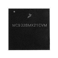
MC9328MX21CVM Freescale, MC9328MX21CVM Datasheet - Page 9

MC9328MX21CVM
Manufacturer Part Number
MC9328MX21CVM
Description
Manufacturer
Freescale
Datasheet
1.MC9328MX21CVM.pdf
(100 pages)
Specifications of MC9328MX21CVM
Operating Temperature (min)
-40C
Operating Temperature (max)
85C
Operating Temperature Classification
Industrial
Mounting
Surface Mount
Lead Free Status / RoHS Status
Compliant
Available stocks
Company
Part Number
Manufacturer
Quantity
Price
Company:
Part Number:
MC9328MX21CVM
Manufacturer:
Freescale Semiconductor
Quantity:
10 000
Company:
Part Number:
MC9328MX21CVMR2
Manufacturer:
Freescale Semiconductor
Quantity:
10 000
Freescale Semiconductor
EXT_DMAGRANT
BMI_READ_REQ
BMI_RXF_FULL
EXT_DMAREQ
BMI_CLK_CS
Signal Name
SLCDC2_D0
BMI_D[15:0]
BMI_WRITE
NF_IO[15:0]
PC_READY
PC_D[15:0]
BMI_READ
PC_A[25:0]
BMI_WAIT
PC_WAIT
PC_CD1
PC_CD2
NF_CLE
NF_ALE
NF_WP
NF_WE
NF_CE
NF_RE
NF_RB
SLCD Data input signal for pass through to SLCD device. This signal is multiplexed with SSI3_FS signal
from SSI3.
BMI bidirectional data bus. Bus width is programmable between 8-bit or 16-bit.These signals are
multiplexed with LD[15:0] and SLCDC_DAT[15:0].
BMI bidirectional clock or chip select signal.This signal is multiplexed with LSCLK of LCDC.
BMI bidirectional signal to indicate read or write access. This is an input signal when the BMI is a slave
and an output signal when BMI is the master of the interface. BMI_WRITE is asserted for write and
negated for read.This signal is muxed with LD[17] of LCDC.
BMI output signal to enable data read from external slave device. This signal is not used and driven high
when BMI is slave.This signal is multiplexed with CONTRAST signal of LCDC.
BMI Read request output signal to external bus master. This signal is active when the data in the TXFIFO
is larger or equal to the data transfer size of a single external BMI access.This signal is muxed with
LD[16] of LCDC.
BMI Receive FIFO full active high output signal to reflect if the RxFIFO reaches water mark value.This
signal is muxed with VSYNC of the LCDC.
BMI Wait—Active low signal to wait for data ready (read cycle) or accepted (write_cycle). Also
multiplexed with VSYNC.
External DMA Request input signal. This signal is multiplexed with CSPI1_RDY.
External DMA Grant output signal. This signal is multiplexed with LD[16] of LCDC and CSPI1_SS1 of
CSPI1.
NAND Flash Command Latch Enable output signal. Multiplexed with PC_POE of PCMCIA.
NAND Flash Chip Enable output signal. This signal is multiplexed with PC_CE1 of PCMCIA.
NAND Flash Write Protect output signal. This signal is multiplexed with PC_CE2 of PCMCIA.
NAND Flash Address Latch Enable output signal. This signal is multiplexed with PC_OE of PCMCIA.
NAND Flash Read Enable output signal. This signal is multiplexed with PC_RW of PCMCIA.
NAND Flash Write Enable output signal. This signal is multiplexed with and PC_BVD2 of PCMCIA.
NAND Flash Ready Busy input signal. This signal is multiplexed with PC_RST of PCMCIA.
NAND Flash Data input and output signals. NF_IO[15:7] signals are multiplexed with A[25:21] and
A[15:13]. NF_IO[7:0] signals are multiplexed with several PCMCIA signals.
PCMCIA Address signals. These signals are multiplexed with A[25:0].
PCMCIA Data input and output signals. These signals are multiplexed with D[15:0].
PCMCIA Card Detect1 input signal. This signal is multiplexed with NFIO[7] signal of NF.
PCMCIA Card Detect2 input signal. This signal is multiplexed with NFIO[6] signal of NF.
PCMCIA Wait input signal to extend current access. This signal is multiplexed with NFIO[5] signal of NF.
PCMCIA Ready input signal indicates card is ready for access. Multiplexed with NFIO[4] signal of NF.
Table 2. i.MX21 Signal Descriptions (Continued)
MC9328MX21 Technical Data, Rev. 3.4
Bus Master Interface (BMI)
NAND Flash Controller
PCMCIA Controller
External DMA
Function/Notes
Signal Descriptions
9


