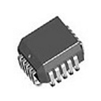
TP3057V National Semiconductor, TP3057V Datasheet - Page 4

TP3057V
Manufacturer Part Number
TP3057V
Description
Manufacturer
National Semiconductor
Type
PCMr
Datasheet
1.TP3057V.pdf
(16 pages)
Specifications of TP3057V
Number Of Channels
1
Gain Control
Adjustable
Number Of Adc's
1
Number Of Dac's
1
Package Type
PLCC
Operating Supply Voltage (typ)
±5V
Number Of Adc Inputs
1
Number Of Dac Outputs
1
Operating Supply Voltage (max)
±5.25V
Operating Supply Voltage (min)
±4.75V
Operating Temperature (max)
85C
Operating Temperature (min)
-40C
Pin Count
20
Mounting
Surface Mount
Lead Free Status / RoHS Status
Not Compliant
Available stocks
Company
Part Number
Manufacturer
Quantity
Price
Part Number:
TP3057V
Manufacturer:
NS/国半
Quantity:
20 000
Part Number:
TP3057V-X
Manufacturer:
NS/国半
Quantity:
20 000
Company:
Part Number:
TP3057V/63SN
Manufacturer:
Texas Instruments
Quantity:
10 000
Company:
Part Number:
TP3057V/NOPB
Manufacturer:
Texas Instruments
Quantity:
10 000
Functional Description
TRANSMIT SECTION
The transmit section input is an operational amplifier with
provision for gain adjustment using two external resistors
see Figure 4 The low noise and wide bandwidth allow gains
in excess of 20 dB across the audio passband to be real-
ized The op amp drives a unity-gain filter consisting of RC
active pre-filter followed by an eighth order switched-ca-
pacitor bandpass filter clocked at 256 kHz The output of
this filter directly drives the encoder sample-and-hold circuit
The A D is of companding type according to
(TP3054) or A-law (TP3057) coding conventions A preci-
sion voltage reference is trimmed in manufacturing to pro-
vide an input overload (t
table of Transmission Characteristics) The FS
pulse controls the sampling of the filter output and then the
successive-approximation encoding cycle begins The 8-bit
code is then loaded into a buffer and shifted out through D
at the next FS
proximately 165
X
pulse The total encoding delay will be ap-
s (due to the transmit filter) plus 125
MAX
) of nominally 2 5V peak (see
(Continued)
X
frame sync
-law
X
s
4
(due to encoding delay) which totals 290
voltage due to the filters or comparator is cancelled by sign
bit integration
RECEIVE SECTION
The receive section consists of an expanding DAC which
drives a fifth order switched-capacitor low pass filter
clocked at 256 kHz The decoder is A-law (TP3057) or
the sin x x attenuation due to the 8 kHz sample hold The
filter is then followed by a 2nd order RC active post-filter
power amplifer capable of driving a 600
7 2 dBm The receive section is unity-gain Upon the occur-
rence of FS
falling edge of the next eight BCLK
the end of the decoder time slot the decoding cycle begins
and 10
total decoder delay is E 10
110
approximately 180 s
-law (TP3054) and the 5th order low pass filter corrects for
s (filter delay) plus 62 5
s later the decoder DAC output is updated The
R
the data at the D
R
s (
s (decoder update) plus
input is clocked in on the
R
(BCLK
frame) which gives
load to a level of
X
s Any offset
) periods At


