LMX2512LQX0967 National Semiconductor, LMX2512LQX0967 Datasheet
LMX2512LQX0967
Specifications of LMX2512LQX0967
Available stocks


Related parts for LMX2512LQX0967

LMX2512LQX0967 Summary of contents
Page 1
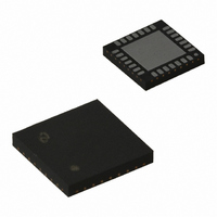
... LMX2502 and LMX2512 feature low current consumption 2.8 V. LMX2502 and LMX2512 are available in a 28-pin leadless leadframe package (LLP). Functional Block Diagram PLLatinum ™ trademark of National Semiconductor Corporation. © 2003 National Semiconductor Corporation Features n Small Size 5 5 0.75 mm 28-Pin LLP Package n RF Synthesizer System Integrated RF VCO ...
Page 2
Connection Diagram NOTE: Analog ground connected through exposed die attached pad. Pin Descriptions Pin Number ...
Page 3
... Ordering Information Part Number RF Min. (MHz) LMX2502LQX1635 1619.62 LMX2502LQ1635 1619.62 LMX2512LQX0967 954.42 LMX2512LQ0967 954.42 LMX2512LQX1065 1052.64 LMX2512LQ1065 1052.64 Part Number Description RF Max. RF Center IF (MHz) (MHz) (MHz) ~ 1635 1649.62 440.76 ~ 1635 1649.62 440.76 ~ 967 979.35 170.76 ~ 967 979.35 170.76 ~ 1065 1077.57 367.20 ~ 1065 1077 ...
Page 4
... Absolute Maximum Ratings Military/Aerospace specified devices are required, please contact the National Semiconductor Sales Office/ Distributors for availability and specifications. Parameter Symbol Ratings Supply Voltage -0 Voltage on any pin V - GND - Storage Temperature T -65 to 150 STG Range Electrical Characteristics Symbol Parameter ...
Page 5
... Note 5: The reference frequency must also be programmed using the OSC_FREQ control bit. For other reference frequencies, please contact National Semiconductor. Note 6: For other frequency ranges, please contact National Semiconductor. Note 7: Lock time is defined as the time difference between the beginning of the frequency transition and the point at which the frequency remains within +/- 1 kHz of the final frequency ...
Page 6
Microwire Interface Timing Diagram www.national.com 6 20068004 ...
Page 7
Functional Description GENERAL DESCRIPTION LMX2502/ highly integrated frequency synthesizer system that generates LO signals for PCS and Cellular CDMA applications. These devices include all the functional blocks of a PLL, RF VCO, prescaler, RF phase detector, and loop ...
Page 8
Functional Description TABLE 2. Power Down Configuration CE Pin RF_EN IF_EN RF Circuitry OFF OFF OFF Don’t care. LOCK DETECT The ...
Page 9
Functional Description MICROWIRE INTERFACE The programmable register set is accessed via the MICROWIRE serial interface. The interface comprises three signal pins: CLK, DATA, and LE (Latch Enable). Serial data (DATA) is clocked into the 24-bit shift register on the rising ...
Page 10
Programming Description GENERAL PROGRAMMING INFORMATION The serial interface has a 24-bit shift register to store the incoming data bits temporarily. The incoming data is loaded into the shift register from MSB to LSB. The data is shifted at the rising ...
Page 11
Programming Description R0 REGISTER The R0 register address bits (R0 [1:0]) are “00”. The SPI_DEF bit selects between using the default IF counter values and user programmable values. The use of the default counter values requires that only words R0 ...
Page 12
... RF_A: Preset divide ratio of binary 3-bit swallow counter (0 ≤ RF_A ≤ 7 for LMX2502, 0 ≤ RF_A ≤ 5 for LMX2512) RF_FN: Preset numerator of binary 11-bit modulus counter (0 ≤ RF_FN = 19.68 MHz Reference oscillator frequency OSC NOTE: For the use of reference frequencies other than those specified, please contact National Semiconductor. www.national.com (Continued) Symbol Function RF_FN ...
Page 13
Programming Description R1 REGISTER The R1 register address bits (R1 [1:0]) are “01”. The IF_FREQ bits selects the default IF frequency applicable to the specific CDMA system. For the LMX2502 the default IF frequency is 440.76 MHz, and for the ...
Page 14
Programming Description R2 REGISTER The R2 Register address bits (R2 [1:0]) are “10”. The IF_CUR [1:0] bits program the IF charge-pump current. Considering the external IF VCO and loop filter, the user can select the amount of IF charge pump ...
Page 15
Programming Description R3 REGISTER The R3 register address bits (R3 [2:0]) are “011”. Register R3 contains the controls for the phase lock bandwidth controls (BW_DUR, BW_CRL, and BW_EN). The duration of the digital controller portion of the bandwidth control is ...
Page 16
Programming Description R4 REGISTER The R4 register address bits (R3 [3:0]) are “0111”. Register R4 is used to set the IF N counters if the default value is not desired. This register is only active if the SPI_DEF bit in ...
Page 17
Programming Description R5 REGISTER The R5 register address bits (R5 [4:0]) are “01111”. Register R5 is used to set the IF_R divider if the default value is not desired. This register is only active if the SPI_DEF bit in register ...
Page 18
... NATIONAL’S PRODUCTS ARE NOT AUTHORIZED FOR USE AS CRITICAL COMPONENTS IN LIFE SUPPORT DEVICES OR SYSTEMS WITHOUT THE EXPRESS WRITTEN APPROVAL OF THE PRESIDENT AND GENERAL COUNSEL OF NATIONAL SEMICONDUCTOR CORPORATION. As used herein: 1. Life support devices or systems are devices or systems which, (a) are intended for surgical implant ...