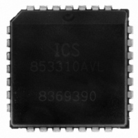
ICS853310AVLF IDT, Integrated Device Technology Inc, ICS853310AVLF Datasheet

ICS853310AVLF
Specifications of ICS853310AVLF
800-1172-5
800-1172
853310AVLF
Available stocks
Related parts for ICS853310AVLF
ICS853310AVLF Summary of contents
Page 1
Integrated Circuit Systems, Inc ENERAL ESCRIPTION The ICS853310 is a low skew, high perfor mance 1-to-8 Differential-to-3.3V LVPECL/ECL HiPerClockS™ ...
Page 2
Integrated Circuit Systems, Inc ABLE IN ESCRIPTIONS ...
Page 3
Integrated Circuit Systems, Inc BSOLUTE AXIMUM ATINGS Supply Voltage, V 4.6V (LVPECL mode Negative Supply Voltage, V -4.6V (LVECL mode Inputs, V (LVPECL mode) -0. Inputs, V (LVECL mode) 0.5V ...
Page 4
Integrated Circuit Systems, Inc. T 2C. LVECL ABLE OWER UPPLY ...
Page 5
Integrated Circuit Systems, Inc. P ARAMETER LVPECL V EE -1.3V ± 0. UTPUT OAD EST IRCUIT nQx Qx nQy Qy tsk( UTPUT KEW nPCLK0, nPCLK1 PCLK0, PCLK1 nQ0:nQ7 Q0:Q7 t ...
Page 6
Integrated Circuit Systems, Inc IRING THE IFFERENTIAL NPUT TO Figure 1A shows an example of the differential input that can be wired to accept single ended LVCMOS levels. The reference voltage level V generated from the device ...
Page 7
Integrated Circuit Systems, Inc. LVPECL LOCK NPUT NTERFACE The PCLK /nPCLK accepts LVPECL, CML, SSTL and other differential signals. Both V and V SWING and V input requirements. Figures show inter- CMR face examples ...
Page 8
Integrated Circuit Systems, Inc ECOMMENDATIONS FOR NUSED I : NPUTS PCLK/nPCLK I : NPUT For applications not requiring the use of a differential input, both the PCLK and nPCLK pins can be left floating. Though not required, ...
Page 9
Integrated Circuit Systems, Inc CHEMATIC XAMPLE Figure 4A shows a schematic example of the ICS853310. In this example, the PCLK0/nPCLK0 input is selected. The decoupling VCC Ohm Ohm LVPECL Driv er R9 ...
Page 10
Integrated Circuit Systems, Inc OWER ROUND AND YPASS APACITOR This section provides a layout guide related to power, ground and placement of bypass capacitors for a high-speed digital IC. This layout guide is a general ...
Page 11
Integrated Circuit Systems, Inc. This section provides information on power dissipation and junction temperature for the ICS853310. Equations and example calculations are also provided. 1. Power Dissipation. The total power dissipation for the ICS853310 is the sum of the core ...
Page 12
Integrated Circuit Systems, Inc. 3. Calculations and Equations. LVPECL output driver circuit and termination are shown in Figure 5. Figure 5. LVPECL Driver Circuit and Termination T o calculate worst case power dissipation into the load, use the following equations ...
Page 13
Integrated Circuit Systems, Inc. θ ABLE VS IR LOW ABLE FOR JA θ θ θ θ θ Multi-Layer PCB, JEDEC Standard Test Boards NOTE: Most modern PCB designs use multi-layered boards. The data in ...
Page 14
Integrated Circuit Systems, Inc ACKAGE UTLINE UFFIX FOR T ABLE Reference Document: JEDEC Publication 95, MS-018 853310AV D - -3.3V LVPECL/ECL F IFFERENTIAL TO PLCC EAD ACKAGE IMENSIONS J E ...
Page 15
Integrated Circuit Systems, Inc ABLE RDERING NFORMATION ...
Page 16
Integrated Circuit Systems, Inc ...


