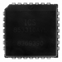
ICS853310AVLF IDT, Integrated Device Technology Inc, ICS853310AVLF Datasheet - Page 8

ICS853310AVLF
Manufacturer Part Number
ICS853310AVLF
Description
IC FANOUT BUFFER LVPECL 28-PLCC
Manufacturer
IDT, Integrated Device Technology Inc
Series
HiPerClockS™r
Type
Fanout Buffer (Distribution), Multiplexerr
Datasheet
1.ICS853310AVLF.pdf
(16 pages)
Specifications of ICS853310AVLF
Number Of Circuits
1
Ratio - Input:output
2:8
Differential - Input:output
Yes/Yes
Input
CML, LVDS, LVPECL, SSTL
Output
ECL, LVPECL
Frequency - Max
2GHz
Voltage - Supply
3 V ~ 3.8 V
Operating Temperature
-40°C ~ 85°C
Mounting Type
Surface Mount
Package / Case
28-PLCC
Frequency-max
2GHz
Lead Free Status / RoHS Status
Lead free / RoHS Compliant
Other names
800-1172
800-1172-5
800-1172
853310AVLF
800-1172-5
800-1172
853310AVLF
Available stocks
Company
Part Number
Manufacturer
Quantity
Price
Company:
Part Number:
ICS853310AVLF
Manufacturer:
IDT, Integrated Device Technology Inc
Quantity:
10 000
Company:
Part Number:
ICS853310AVLFT
Manufacturer:
IDT, Integrated Device Technology Inc
Quantity:
10 000
R
I
PCLK/nPCLK I
For applications not requiring the use of a differential input,
both the PCLK and nPCLK pins can be left floating. Though
not required, but for additional protection, a 1kΩ resistor can
be tied from PCLK to ground.
LVCMOS C
All control pins have internal pull-ups or pull-downs; additional
resistance is not required but can be added for additional
protection. A 1kΩ resistor can be used.
853310AV
T
The clock layout topology shown below is a typical termi-
nation for LVPECL outputs. The two different layouts men-
tioned are recommended only as guidelines.
FOUT and nFOUT are low impedance follower outputs that
generate ECL/LVPECL compatible outputs. Therefore, ter-
minating resistors (DC current path to ground) or current
sources must be used for functionality. These outputs are
designed to drive 50Ω transmission lines. Matched imped-
NPUTS
RTT =
ECOMMENDATIONS FOR
ERMINATION FOR
:
((V
FOUT
F
OH
IGURE
ONTROL
+ V
NPUT
OL
Integrated
Circuit
Systems, Inc.
3A. LVPECL O
) / (V
P
1
:
INS
LVPECL O
CC
:
Z
Z
– 2)) – 2
o
o
= 50Ω
= 50Ω
U
NUSED
Z
o
50Ω
UTPUT
UTPUTS
I
NPUT AND
T
ERMINATION
RTT
www.icst.com/products/hiperclocks.html
50Ω
D
V
CC
IFFERENTIAL
O
FIN
- 2V
UTPUT
P
8
INS
O
LVPECL O
All unused LVPECL outputs can be left floating. We
recommend that there is no trace attached. Both sides of the
differential output pair should either be left floating or
terminated.
ance techniques should be used to maximize operating
frequency and minimize signal distortion. Figures 3A and
3B show two different layouts which are recommended only
as guidelines. Other suitable clock layouts may exist and it
would be recommended that the board designers simulate
to guarantee compatibility across all printed circuit and
clock component process variations.
-
TO
UTPUTS
-3.3V LVPECL/ECL F
FOUT
F
:
UTPUT
IGURE
3B. LVPECL O
Z
Z
o
o
= 50Ω
= 50Ω
125Ω
84Ω
UTPUT
L
OW
ICS853310
3.3V
T
ANOUT
125Ω
84Ω
S
ERMINATION
REV. A OCTOBER 27, 2008
KEW
FIN
, 1-
B
UFFER
TO
-8


