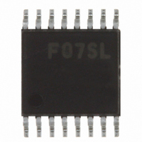
MB15F07SLPFV1-BND-6E1 Fujitsu Semiconductor America Inc, MB15F07SLPFV1-BND-6E1 Datasheet - Page 11

MB15F07SLPFV1-BND-6E1
Manufacturer Part Number
MB15F07SLPFV1-BND-6E1
Description
SYNTHESZR PLL 1.1GHZ DUAL 16SSOP
Manufacturer
Fujitsu Semiconductor America Inc
Type
Clock/Frequency Synthesizer (RF/IF), Prescalerr
Datasheet
1.MB15F07SLPFV1-BND-6E1.pdf
(27 pages)
Specifications of MB15F07SLPFV1-BND-6E1
Pll
Yes
Input
Clock
Output
Clock
Number Of Circuits
1
Ratio - Input:output
2:1
Differential - Input:output
Yes/No
Frequency - Max
1.1GHz
Divider/multiplier
Yes/No
Voltage - Supply
2.4 V ~ 3.6 V
Operating Temperature
-40°C ~ 85°C
Mounting Type
Surface Mount
Package / Case
16-SSOP
Frequency-max
1.1GHz
Lead Free Status / RoHS Status
Lead free / RoHS Compliant
Other names
865-1003-6
Available stocks
Company
Part Number
Manufacturer
Quantity
Price
Company:
Part Number:
MB15F07SLPFV1-BND-6E1
Manufacturer:
Fujitsu
Quantity:
3 000
Table 8. LD/fout Output Select Data Setting
Table 9. Charge Pump Current Setting
Power Saving Mode (Intermittent Mode Control Circuit)
Table 10. PS Pin Setting
The intermittent mode control circuit reduces the PLL power consumption.
By setting the PS pin low, the device enters into the power saving mode, reducing the current consumption. See
the Electrical Characteristics chart for the specific value.
The phase detector output, Do, becomes high impedance.
For the dual PLL, the lock detector, LD, is as shown in the LD Output Logic table.
Setting the PS pin high, releases the power saving mode, and the device works normally.
The intermittent mode control circuit also ensures a smooth startup when the device returns to normal operation.
When the PLL is returned to normal operation, the phase comparator output signal is unpredictable. This is because
of the unknown relationship between the comparison frequency (fp) and the reference frequency (fr) which can
cause a major change in the comparator output, resulting in a VCO frequency jump and an increase in lockup time.
To prevent a major VCO frequency jump, the intermittent mode control circuit limits the magnitude of the error signal
from the phase detector when it returns to normal operation.
Notes: When power (V
PS pin
LDS
CS
H
H
H
L
L
L
(1) PS = L (power saving mode) at Power-ON
(2) Set serial data
(3) Release power saving mode (PS:
PS pins must be set at “L” for Power-ON .
fout (fr
LD signal
Normal mode
Power saving mode
1
/fr
V
Clock
Data
LE
PS
1 s
2
CC
, fp
CC
LD/fout output signal
) is first applied, the device must be in standby mode, PS = Low, for at least 1 s.
1
later after power supply remains stable (V
/fp
Current value
2
) signals
Status
6.0 mA
1.5 mA
OFF
(1)
“
L
”
“
H
”
) 100 ns later after setting serial data.
tv
1 s
(2)
CC
ON
2.2 V).
(3)
tps
100 ns
MB15F07SL
11


