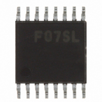
MB15F07SLPFV1-BND-6E1 Fujitsu Semiconductor America Inc, MB15F07SLPFV1-BND-6E1 Datasheet - Page 3

MB15F07SLPFV1-BND-6E1
Manufacturer Part Number
MB15F07SLPFV1-BND-6E1
Description
SYNTHESZR PLL 1.1GHZ DUAL 16SSOP
Manufacturer
Fujitsu Semiconductor America Inc
Type
Clock/Frequency Synthesizer (RF/IF), Prescalerr
Datasheet
1.MB15F07SLPFV1-BND-6E1.pdf
(27 pages)
Specifications of MB15F07SLPFV1-BND-6E1
Pll
Yes
Input
Clock
Output
Clock
Number Of Circuits
1
Ratio - Input:output
2:1
Differential - Input:output
Yes/No
Frequency - Max
1.1GHz
Divider/multiplier
Yes/No
Voltage - Supply
2.4 V ~ 3.6 V
Operating Temperature
-40°C ~ 85°C
Mounting Type
Surface Mount
Package / Case
16-SSOP
Frequency-max
1.1GHz
Lead Free Status / RoHS Status
Lead free / RoHS Compliant
Other names
865-1003-6
Available stocks
Company
Part Number
Manufacturer
Quantity
Price
Company:
Part Number:
MB15F07SLPFV1-BND-6E1
Manufacturer:
Fujitsu
Quantity:
3 000
SSOP-16 BCC-16
PIN DESCRIPTIONS
10
11
12
13
14
15
16
1
2
3
4
5
6
7
8
9
Pin no.
16
10
11
12
13
14
15
1
2
3
4
5
6
7
8
9
LD/fout
OSC
name
GND
GND
Clock
Xfin
Data
V
V
PS
Do
Do
PS
Pin
fin
fin
LE
CC1
CC2
1
2
1
2
1
2
2
IN
2
1
I/O
O
O
O
–
–
–
–
I
I
I
I
I
I
I
I
I
Ground for PLL 2 section.
The programmable reference divider input. TCXO should be connected
with a AC coupling capacitor.
Ground for the PLL 1 section.
Prescaler input pin for the PLL 1.
Connection to an external VCO should be via AC coupling.
Power supply voltage input pin for the PLL 1 section.
Lock detect signal output (LD)/phase comparator monitoring
output (fout).
The output signal is selected by LDS bit in a serial data.
LDS bit = “H” ; outputs fout signal
LDS bit = “L” ; outputs LD signal
Power saving mode control for the PLL 1 section. This pin must be set
at “L” during Power-ON. (Open is prohibited.)
PS
PS
Charge pump output for the PLL 1 section.
Phase characteristics of the phase detector can be selected via
programming of the FC-bit.
Charge pump output for the PLL 2 section.
Phase characteristics of the phase detector can be selected via
programming of the FC-bit.
Power saving mode control for the PLL 2 section. This pin must be set
at “L” during Power-ON. (Open is prohibited.)
PS
PS
Prescaler complementary input for the PLL 2 section.
This pin should be grounded via a capacitor.
Power supply voltage input pin for the PLL 2 section, the shift register and
the oscillator input buffer. When power is OFF, latched data of PLL 2 is lost.
Prescaler input pin for the PLL 2.
Connection to an external VCO should be via AC coupling.
Load enable signal inpunt (with a schmitt trigger input buffer.)
When the LE bit is set “H”, data in the shift register is transferred to the
corresponding latch according to the control bit in the serial data.
Serial data input (with a schmitt trigger input buffer.)
Data is transferred to the corresponding latch (PLL 1-ref counter, PLL 1-
prog. counter, PLL 2-ref. counter, PLL 2-prog. counter) according to the
control bit in the serial data.
Clock input for the 23-bit shift register (with a schmitt trigger input buffer.)
One bit of data is shifted into the shift register on a rising edge of the clock.
1
1
2
2
= “H” ; Normal mode
= “L” ; Power saving mode
= “H” ; Normal mode
= “L” ; Power saving mode
Descriptions
MB15F07SL
3


