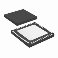
LMK03033CISQE/NOPB National Semiconductor, LMK03033CISQE/NOPB Datasheet - Page 14

LMK03033CISQE/NOPB
Manufacturer Part Number
LMK03033CISQE/NOPB
Description
IC CLOCK CONDITIONER PREC 48LLP
Manufacturer
National Semiconductor
Type
Clock Conditionerr
Datasheet
1.LMK03000DISQENOPB.pdf
(30 pages)
Specifications of LMK03033CISQE/NOPB
Pll
Yes
Input
Clock
Output
LVDS, LVPECL
Number Of Circuits
1
Ratio - Input:output
1:4
Differential - Input:output
Yes/Yes
Frequency - Max
2.1GHz
Divider/multiplier
Yes/No
Voltage - Supply
3.15 V ~ 3.45 V
Operating Temperature
-40°C ~ 85°C
Mounting Type
Surface Mount
Package / Case
48-LLP
Frequency-max
2.1GHz
Lead Free Status / RoHS Status
Lead free / RoHS Compliant
Other names
LMK03033CISQETR
Available stocks
Company
Part Number
Manufacturer
Quantity
Price
Company:
Part Number:
LMK03033CISQE/NOPB
Manufacturer:
NS
Quantity:
464
Part Number:
LMK03033CISQE/NOPB
Manufacturer:
TI/德州仪器
Quantity:
20 000
www.national.com
2.0 General Programming
Information
The LMK03000 family of devices are programmed using sev-
eral 32-bit registers which control the device's operation. The
registers consist of a data field and an address field. The last
4 register bits, ADDR[3:0] form the address field. The remain-
ing 28 bits form the data field DATA[27:0].
During programming, LEuWire is low and serial data is
clocked in on the rising edge of CLKuWire (MSB first). When
LE goes high, data is transferred to the register bank selected
by the address field. Only registers R0 to R7, R11, and R13
to R15 need to be programmed for proper device operation.
For the frequency calibration algorithm to work properly OS-
Cin must be driven by a valid signal when R15 is programmed.
Any changes to the PLL R divider or OSCin require R15 to be
programmed again to activate the frequency calibration rou-
tine.
2.1 RECOMMENDED PROGRAMMING SEQUENCE
The recommended programming sequence involves pro-
gramming R0 with the reset bit set (RESET = 1) to ensure the
device is in a default state. It is not necessary to program R0
again, but if R0 is programmed again, the reset bit is pro-
grammed clear (RESET = 0). Registers are programmed in
order with R15 being the last register programmed. An ex-
ample programming sequence is shown below.
•
•
•
•
•
•
•
•
Program R0 with the reset bit set (RESET = 1). This
ensures the device is in a default state. When the reset bit
is set in R0, the other R0 bits are ignored.
— If R0 is programmed again, the reset bit is programmed
Program R0 to R7 as necessary with desired clocks with
appropriate enable, mux, divider, and delay settings.
Program R8 for optimum phase noise performance.
Program R9 with Vboost setting if necessary. Optional,
only needed to set Vboost = 1.
Program R11 with DIV4 setting if necessary.
Program R13 with oscillator input frequency and internal
loop filter values
Program R14 with Fout enable bit, global clock output bit,
power down setting, PLL mux setting, and PLL R divider.
Program R15 with PLL charge pump gain, VCO divider,
and PLL N divider. Also starts frequency calibration
routine.
clear (RESET = 0).
14


