MC100EL34DG ON Semiconductor, MC100EL34DG Datasheet
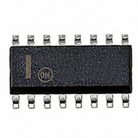
IC CLOCK GEN ECL 2/4/8 16SOIC

MC100EL34DG

Manufacturer Part Number
MC100EL34DG
Description
IC CLOCK GEN ECL 2/4/8 16SOIC
Manufacturer
ON Semiconductor
Series
100ELr
Type
Clock Generatorr
Datasheet

Specifications of MC100EL34DG

Pll
No
Input
NECL, PECL
Output
ECL
Number Of Circuits
1
Ratio - Input:output
1:3
Differential - Input:output
Yes/Yes
Frequency - Max
1.1GHz
Divider/multiplier
Yes/No
Voltage - Supply
±4.2 V ~ 5.7 V
Operating Temperature
-40°C ~ 85°C
Mounting Type
Surface Mount
Package / Case
16-SOIC (3.9mm Width)
Frequency-max
1.1GHz
Mounting Style
SMD/SMT
Lead Free Status / RoHS Status
Lead free / RoHS Compliant
Other names
MC100EL34DGOS

Available stocks

Company
Part Number
Manufacturer
Quantity
Price
Part Number:
MC100EL34DG
Manufacturer:
ON Semiconductor
Quantity:
8
MC10EL34, MC100EL34
5V ECL ÷2, ÷4, ÷8 Clock
Generation Chip
Description
designed explicitly for low skew clock generation applications. The
internal dividers are synchronous to each other, therefore, the common
output edges are all precisely aligned. The V
generated voltage supply, is available to this device only. For
single-ended input conditions, the unused differential input is
connected to V
rebias AC coupled inputs. When used, decouple V
0.01 mF capacitor and limit current sourcing or sinking to 0.5 mA.
When not used, V
dividers will only be enabled/disabled when the internal clock is
already in the LOW state. This avoids any chance of generating a runt
clock pulse on the internal clock when the device is enabled/disabled
as can happen with an asynchronous control. An internal runt pulse
could lead to losing synchronization between the internal divider
stages. The internal enable flip−flop is clocked on the falling edge of
the input clock, therefore, all associated specification limits are
referenced to the negative edge of the clock input.
master reset (MR) input allows for the synchronization of the internal
dividers, as well as multiple EL34s in a system.
Features
*For additional information on our Pb−Free strategy and soldering details, please
© Semiconductor Components Industries, LLC, 2006
November, 2006 − Rev. 10
download the ON Semiconductor Soldering and Mounting Techniques
Reference Manual, SOLDERRM/D.
The MC10/100EL34 is a low skew ÷2, ÷4, ÷8 clock generation chip
The common enable (EN) is synchronous so that the internal
Upon startup, the internal flip-flops will attain a random state; the
The 100 Series contains temperature compensation.
V
V
50 ps Output-to-Output Skew
Synchronous Enable/Disable
Master Reset for Synchronization
PECL Mode Operating Range:
NECL Mode Operating Range:
Internal Input 75 kW Pulldown Resistors on CLK(s), EN, and MR
Pb−Free Packages are Available*
CC
CC
= 4.2 V to 5.7 V with V
= 0 V with V
BB
BB
as a switching reference voltage. V
EE
should be left open.
= −4.2 V to −5.7 V
EE
= 0 V
BB
BB
pin, an internally
and V
BB
may also
1
CC
via a
See detailed ordering and shipping information in the package
dimensions section on page 7 of this data sheet.
16
1
*For additional marking information, refer to
Application Note AND8002/D.
AWLYWW
10EL34G
ORDERING INFORMATION
A
WL
YY
WW
G
MARKING DIAGRAMS*
http://onsemi.com
16
= Assembly Location
= Wafer Lot
= Year
= Work Week
= Pb−Free Package
CASE 751B
D SUFFIX
SO−16
1
Publication Order Number:
16
1
100EL34G
AWLYWW
MC10EL34/D

Related parts for MC100EL34DG

MC100EL34DG Summary of contents

Page 1

... Internal Input 75 kW Pulldown Resistors on CLK(s), EN, and MR • Pb−Free Packages are Available* *For additional information on our Pb−Free strategy and soldering details, please download the ON Semiconductor Soldering and Mounting Techniques Reference Manual, SOLDERRM/D. © Semiconductor Components Industries, LLC, 2006 November, 2006 − Rev. 10 ...

Page 2

CLK CLK ÷2 ÷ *All V pins ...

Page 3

Table 4. MAXIMUM RATINGS Symbol Parameter V PECL Mode Power Supply CC V NECL Mode Power Supply EE V PECL Mode Input Voltage I NECL Mode Input Voltage I Output Current out I V Sink/Source Operating Temperature ...

Page 4

Table 6. 10EL SERIES NECL DC CHARACTERISTICS Symbol Characteristic I Power Supply Current EE V Output HIGH Voltage (Note Output LOW Voltage (Note Input HIGH Voltage (Single−Ended Input LOW Voltage (Single−Ended) IL ...

Page 5

Table 8. 100EL SERIES NECL DC CHARACTERISTICS Symbol Characteristic I Power Supply Current EE V Output HIGH Voltage (Note 12 Output LOW Voltage (Note 12 Input HIGH Voltage (Single−Ended Input LOW Voltage (Single−Ended) IL ...

Page 6

There are two distinct functional relationships between the Master Reset and Clock: MR CLK CASE 1: If the MR is de−asserted (H−L), while the Clock is still high, the outputs will follow the first ensuing clock ...

Page 7

... Application Note AND8020/D − Termination of ECL Logic Devices.) ORDERING INFORMATION Device MC10EL34D MC10EL34DG MC10EL34DR2 MC10EL34DR2G MC100EL34D MC100EL34DG MC100EL34DR2 MC100EL34DR2G †For information on tape and reel specifications, including part orientation and tape sizes, please refer to our Tape and Reel Packaging Specifications Brochure, BRD8011/D. Resource Reference of Application Notes AN1405/D AN1406/D ...

Page 8

... Opportunity/Affirmative Action Employer. This literature is subject to all applicable copyright laws and is not for resale in any manner. PUBLICATION ORDERING INFORMATION LITERATURE FULFILLMENT: Literature Distribution Center for ON Semiconductor P.O. Box 5163, Denver, Colorado 80217 USA Phone: 303−675−2175 or 800−344−3860 Toll Free USA/Canada Fax: 303− ...

Related keywords