AD9901KP-REEL Analog Devices Inc, AD9901KP-REEL Datasheet - Page 4
AD9901KP-REEL
Manufacturer Part Number
AD9901KP-REEL
Description
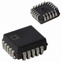
IC PHASE/FREQ DISCRIMR 20-PLCC
Manufacturer
Analog Devices Inc
Type
Digital Phase/Frequency Discriminatorr
Datasheet
1.AD9901KPZ.pdf
(8 pages)
Specifications of AD9901KP-REEL
Rohs Status
RoHS non-compliant
Pll
Yes
Input
CMOS, ECL, TTL
Output
CMOS, ECL, TTL
Number Of Circuits
1
Ratio - Input:output
2:1
Differential - Input:output
Yes/Yes
Frequency - Max
200MHz
Voltage - Supply
5V
Operating Temperature
0°C ~ 70°C
Mounting Type
Surface Mount
Package / Case
20-PLCC
Frequency-max
200MHz
Available stocks
Company
Part Number
Manufacturer
Quantity
Price
Company:

Part Number:
AD9901KP-REEL
Manufacturer:
ADI
Quantity:
500


AD9901
TTL/CMOS MODE FUNCTIONAL PIN DESCRIPTIONS
GROUND
+V
BIAS
VCO INPUT
OUTPUT
R
OUTPUT
REFERENCE
INPUT
SET
S
Figure 1. TTL Mode (Based on DIP Pinouts)
AD9901
BIAS
+V
S
Ground connections for AD9901. Connect
all grounds together and to low impedance
ground plane as close to the device as
possible.
Positive supply connection; nominally +5.0 V
for TTL operation.
Connect to +V
TTL compatible input; normally connected
to the VCO output signal. VCO INPUT and
REFERENCE INPUT are equivalent to one
another.
The noninverted output. In TTL/CMOS
mode, the output swing is approximately
+3.2 V to +5 V.
External R
through the R
mum full-scale output current. R
be connected to ground through an external
resistor in TTL mode. I
I
The inverted output. In TTL/CMOS mode,
the output swing is approximately +3.2 V to
+5 V.
TTL compatible input, normally connected
to the reference input signal. The VCO
INPUT and the REFERENCE INPUT are
equivalent.
LOAD
REFERENCE
OUTPUT
(max).
SET
INPUT
VCO
+V
SET
connection. The current
S
S
(+5 V) for TTL operation.
OUTPUT
OUTPUT
resistor is equal to the maxi-
R3
R2
+V
+V
SET
S
S
= 0.47 V/R
R
SET
R1
+V
REG
S
SET
should
SET
=
–4–
ECL MODE FUNCTIONAL PIN DESCRIPTIONS
–V
BIAS
VCO INPUT
VCO INPUT
OUTPUT
GROUND
R
OUTPUT
REFERENCE
INPUT
REFERENCE
INPUT
SET
S
Figure 2. ECL Mode (Based on DIP Pinouts)
REFERENCE
INPUT
–V
AD9901
S
BIAS
Negative supply connection, nominally
–5.2 V for ECL operation.
Connect to –5.2 V for ECL operation.
Inverted side of ECL compatible differential
input, normally connected to the VCO output
signal.
Noninverted side of ECL-compatible
differential input, normally connected to the
VCO output signal.
The noninverted output. In ECL mode, the
output swing is approximately 0 V to –1.8 V.
Ground connections for AD9901. Connect
all grounds together and to low-impedance
ground plane as close to the device as
possible.
External R
through the R
mum full-scale output current. R
be connected to –V
resistor in ECL mode. I
I
The inverted output. In ECL mode, the out-
put swing is approximately 0 V to –1.8 V.
Noninverted side of ECL-compatible
differential input, normally connected to the
reference input signal. The VCO INPUT and
the REFERENCE INPUT are equivalent to
one another.
Inverted side of ECL-compatible differential
input, normally connected to the reference
input signal. The VCO INPUT and the
REFERENCE INPUT are equivalent.
LOAD
REFERENCE
INPUT
VCO
INPUT
(max).
INPUT
VCO
SET
–V
S
–V
SET
connection. The current
S
OUTPUT
resistor is equal to the maxi-
OUTPUT
S
through an external
R2
R3
SET
= 0.47 V/R
R
SET
R1
REG
–V
SET
S
should
REV. B
SET
=
Related parts for AD9901KP-REEL
Image
Part Number
Description
Manufacturer
Datasheet
Request
R

Part Number:
Description:
IC PHS/FREQ DISCRIMINATOR 20PLCC
Manufacturer:
Analog Devices Inc
Datasheet:

Part Number:
Description:
±1.7g Dual-Axis IMEMS Accelerometer Evaluation Board
Manufacturer:
Analog Devices Inc
Datasheet:

Part Number:
Description:
Inertial Sensor Evaluation System
Manufacturer:
Analog Devices Inc
Datasheet:
Part Number:
Description:
Manufacturer:
Analog Devices Inc
Datasheet:
Part Number:
Description:
Manufacturer:
Analog Devices Inc
Datasheet:
Part Number:
Description:
Manufacturer:
Analog Devices Inc
Datasheet:
Part Number:
Description:
Manufacturer:
Analog Devices Inc
Datasheet:
Part Number:
Description:
Manufacturer:
Analog Devices Inc
Datasheet:
Part Number:
Description:
Manufacturer:
Analog Devices Inc
Datasheet:
Part Number:
Description:
Manufacturer:
Analog Devices Inc
Datasheet:
Part Number:
Description:
Manufacturer:
Analog Devices Inc
Datasheet:
Part Number:
Description:
Manufacturer:
Analog Devices Inc
Datasheet:
Part Number:
Description:
Manufacturer:
Analog Devices Inc
Datasheet: