AD9901KP-REEL Analog Devices Inc, AD9901KP-REEL Datasheet - Page 6
AD9901KP-REEL
Manufacturer Part Number
AD9901KP-REEL
Description
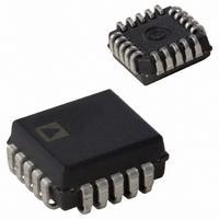
IC PHASE/FREQ DISCRIMR 20-PLCC
Manufacturer
Analog Devices Inc
Type
Digital Phase/Frequency Discriminatorr
Datasheet
1.AD9901KPZ.pdf
(8 pages)
Specifications of AD9901KP-REEL
Rohs Status
RoHS non-compliant
Pll
Yes
Input
CMOS, ECL, TTL
Output
CMOS, ECL, TTL
Number Of Circuits
1
Ratio - Input:output
2:1
Differential - Input:output
Yes/Yes
Frequency - Max
200MHz
Voltage - Supply
5V
Operating Temperature
0°C ~ 70°C
Mounting Type
Surface Mount
Package / Case
20-PLCC
Frequency-max
200MHz
Available stocks
Company
Part Number
Manufacturer
Quantity
Price
Company:

Part Number:
AD9901KP-REEL
Manufacturer:
ADI
Quantity:
500


AD9901
THEORY OF OPERATION
A phase detector is one of three basic components of a phase-
locked loop (PLL); the other two are a filter and a tunable oscil-
lator. A basic PLL control system is shown in Figure 3.
The function of the phase detector is to generate an error signal
that is used to retune the oscillator frequency whenever its out-
put deviates from a reference input signal. The two most com-
mon methods of implementing phase detectors are (1) an analog
mixer and (2) a family of sequential logic circuits known as
digital phase detectors.
The AD9901 is a digital phase detector. As illustrated in the
block diagram of the unit, straightforward sequential logic de-
sign is used. The main components include four “D” flip-flops,
an exclusive-OR gate (XOR) and some combinational output
logic. The circuit operates in two distinct modes: as a linear
phase detector and as a frequency discriminator.
When the reference and oscillator are very close in frequency,
only the phase detection circuit is active. If the two inputs are
substantially different in frequency, the frequency discrimina-
tion circuit overrides the phase detector portion to drive the
oscillator frequency toward the reference frequency and put it
within range of the phase detector.
Input signals to the AD9901 are pulse trains, and its output
duty cycle is proportional to the phase difference of the oscilla-
tor and reference inputs. Figures 4, 5 and 6 illustrate, respec-
tively, the input/output relationships at lock; with the
REFERENCE
Figure 4. AD9901 Timing Waveforms at “Lock”
INPUT
Figure 3. Phase-Locked Loop Control System
Figure 5. Timing Waveforms (
AD9901
OSCILLATOR
OSCILLATOR
OSCILLATOR
OSCILLATOR
REFERENCE
REFERENCE
REFERENCE
REFERENCE
FLIP-FLOP
FLIP-FLOP
FLIP-FLOP
FLIP-FLOP
XORGATE
XORGATE
OUTPUT
OUTPUT
OUTPUT
OUTPUT
OUTPUT
OUTPUT
INPUT
INPUT
INPUT
INPUT
DC MEAN VALUE
DC MEAN VALUE
FILTER
PASS
LOW-
1/N
OPTIONAL 1/N PRESCALER
TYPICAL OF DIGITAL PLLs
VCO
OUT
Leads
OSCILLATOR
OUTPUT
IN
)
–6–
oscillator leading the reference frequency; and with the oscillator
lagging. This output pulse train is low-pass filtered to extract the
dc mean value [K (
stant (phase gain).
At or near lock (Figures 4, 5 and 6), only the two input flip-
flops and the exclusive-OR gate (the phase detection circuit) are
active. The input flip-flops divide both the reference and oscilla-
tor frequencies by a factor of two. This insures that inputs to the
exclusive-OR are square waves, regardless of the input duty
cycles of the frequencies being compared. This division-by-two
also moves the nonlinear detection range to the ends of the
range rather than near lock, which is the case with conventional
digital phase detectors.
Figure 7 illustrates the constant gain near lock.
When the two square waves are combined by the XOR, the
output has a 50% duty cycle if the reference and oscillator in-
puts are exactly 180 out of phase; under these conditions, the
AD9901 is operating in a locked mode. Any shift in the phase
relationship between these input signals causes a change in the
output duty cycle. Near lock, the frequency discriminator flip-
flops provide constant HIGH levels to gate the XOR output to
the final output.
The duty cycle of the AD9901 is a direct measure of the phase
difference between the two input signals when the unit is near
lock. The transfer function can be stated as [K (
where K is the allowable output voltage range of the AD9901
divided by 2 .
For a typical output swing of 1.8 V, the transfer function can be
stated as (1.8 V/2
tionship of the dc mean value of the AD9901 output as a func-
tion of the phase difference of the two inputs.
Figure 6. Timing Waveforms (
2
1
0
–2
OSCILLATOR
OSCILLATOR
REFERENCE
REFERENCE
FLIP-FLOP
FLIP-FLOP
XORGATE
OUTPUT
OUTPUT
OUTPUT
INPUT
INPUT
Figure 7. Phase Gain Plot
= 0.285 V/RAD). Figure 7 shows the rela-
I
PHASE DIFFERENCE AT INPUTS
–
DC MEAN VALUE
O
)] where K is a proportionality con-
F
O
= 200MHz
F
O
–
= 70MHz
TYPICAL PHASE DETECTOR
GAIN IS 0.2865V/RAD
V
OUT
OUT
= 1.8V
Lags
I
F
–
O
= 50MHz
O
](V/RAD),
IN
)
0
REV. B
Related parts for AD9901KP-REEL
Image
Part Number
Description
Manufacturer
Datasheet
Request
R

Part Number:
Description:
IC PHS/FREQ DISCRIMINATOR 20PLCC
Manufacturer:
Analog Devices Inc
Datasheet:

Part Number:
Description:
±1.7g Dual-Axis IMEMS Accelerometer Evaluation Board
Manufacturer:
Analog Devices Inc
Datasheet:

Part Number:
Description:
Inertial Sensor Evaluation System
Manufacturer:
Analog Devices Inc
Datasheet:
Part Number:
Description:
Manufacturer:
Analog Devices Inc
Datasheet:
Part Number:
Description:
Manufacturer:
Analog Devices Inc
Datasheet:
Part Number:
Description:
Manufacturer:
Analog Devices Inc
Datasheet:
Part Number:
Description:
Manufacturer:
Analog Devices Inc
Datasheet:
Part Number:
Description:
Manufacturer:
Analog Devices Inc
Datasheet:
Part Number:
Description:
Manufacturer:
Analog Devices Inc
Datasheet:
Part Number:
Description:
Manufacturer:
Analog Devices Inc
Datasheet:
Part Number:
Description:
Manufacturer:
Analog Devices Inc
Datasheet:
Part Number:
Description:
Manufacturer:
Analog Devices Inc
Datasheet:
Part Number:
Description:
Manufacturer:
Analog Devices Inc
Datasheet: