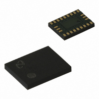
LMX2332USLBX National Semiconductor, LMX2332USLBX Datasheet - Page 40

LMX2332USLBX
Manufacturer Part Number
LMX2332USLBX
Description
IC FREQ SYNTH DUAL 24LAMINATECSP
Manufacturer
National Semiconductor
Series
PLLatinum™r
Type
PLL Frequency Synthesizerr
Datasheet
1.LMX2330UTM.pdf
(49 pages)
Specifications of LMX2332USLBX
Pll
Yes with Bypass
Input
CMOS, TTL
Output
CMOS
Number Of Circuits
1
Ratio - Input:output
3:1
Differential - Input:output
Yes/No
Frequency - Max
1.2GHz, 600MHz
Divider/multiplier
Yes/No
Voltage - Supply
2.7 V ~ 5.5 V
Operating Temperature
-40°C ~ 85°C
Mounting Type
Surface Mount
Package / Case
24-Laminate CSP
Frequency-max
1.2GHz
Lead Free Status / RoHS Status
Contains lead / RoHS non-compliant
Other names
LMX2332USLBXTR
www.national.com
2.0 Programming Description
2.1 MICROWIRE INTERFACE
The 22-bit shift register is loaded via the MICROWIRE interface. The shift register consists of a 20-bit Data[19:0] Field and a 2-bit
Address[1:0] Field as shown below. The Address Field is used to decode the internal control register address. When LE
transitions HIGH, data stored in the shift register is loaded into one of 4 control registers depending on the state of the address
bits. The MSB of Data is loaded in first. The Data Field assignments are shown in Section 2.3 CONTROL REGISTER CONTENT
MAP.
2.2 CONTROL REGISTER LOCATION
The address bits Address[1:0] decode the internal register address. The table below shows how the address bits are mapped into
the target control register.
2.3 CONTROL REGISTER CONTENT MAP
The control register content map describes how the bits within each control register are allocated to specific control functions.
MSB
21
Address[1:0]
0
0
1
1
Data[19:0]
Field
0
1
0
1
40
2 1
Register
Target
RF R
RF N
IF R
IF N
Address[1:0]
LSB
0


