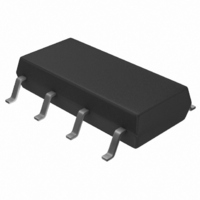
S-35190A-J8T1G Seiko Instruments, S-35190A-J8T1G Datasheet - Page 18

S-35190A-J8T1G
Manufacturer Part Number
S-35190A-J8T1G
Description
IC REAL TIME CLOCK 3WIRE 8-SOP
Manufacturer
Seiko Instruments
Type
Clock/Calendarr
Datasheet
1.S-35190A-J8T1G.pdf
(55 pages)
Specifications of S-35190A-J8T1G
Time Format
HH:MM:SS (12/24 hr)
Date Format
YY-MM-DD-dd
Interface
3-Wire Serial
Voltage - Supply
1.3 V ~ 5.5 V
Operating Temperature
-40°C ~ 85°C
Mounting Type
Surface Mount
Package / Case
8-SOP
Lead Free Status / RoHS Status
Lead free / RoHS Compliant
Memory Size
-
Available stocks
Company
Part Number
Manufacturer
Quantity
Price
Company:
Part Number:
S-35190A-J8T1G
Manufacturer:
SEIKO
Quantity:
2 246
Part Number:
S-35190A-J8T1G
Manufacturer:
SEIKO
Quantity:
20 000
18
3-WIRE REAL-TIME CLOCK
S-35190A
Power-on Detection Circuit and Register Status
The power-on detection circuit operates by power-on the S-35190A, as a result each register is cleared; each register is set
as follows.
“1” is set in the POC flag (B0 in the status register 1) to indicate that power has been applied. To correct the oscillation
frequency, the status register 2 goes in the mode the output of user-set frequency, so that 1 Hz clock pulse is output from
the INT pin. When “1” is set in the POC flag, be sure to initialize. The POC flag is set to “0” due to initialization so that the
output of user-set frequency mode is cleared. (Refer to “ Register Status After Initialization ”.)
For the regular operation of power-on detection circuit, as seen in Figure 22 , the period to power-up the S-35190A is that
the voltage reaches 1.3 V within 10 ms after setting the IC’s power supply voltage at 0 V. When the power-on detection
circuit is not working normally is; the POC flag (B0 in the status register) is not in “1”, or 1 Hz is not output from the INT pin.
In this case, power-on the S-35190A once again because the internal data may be in the indefinite status.
Do not transmit data immediately after power-on at least 0.5 sec because the power-on detection circuit is operating.
Real-time data register :
Status register 1 :
Status register 2 :
INT register 1 :
INT register 2 :
Clock correction register :
Free register :
*1. 0 V indicates that there are no potential differences between the VDD
pin and VSS pin of the S-35190A.
Figure 22 How to Raise the Power Supply Voltage
“01h”
“80h”
“80h”
“00h”
“00h”
“00h”
00 (Y), 01 (M), 01 (D), 0 (day of the week), 00 (H), 00 (M), 00 (S)
Seiko Instruments Inc.
Within 10 ms
1.3 V
0 V
*1
Rev.3.0
_00


