MM58167BN National Semiconductor, MM58167BN Datasheet
MM58167BN
Specifications of MM58167BN
Available stocks


Related parts for MM58167BN

MM58167BN Summary of contents
Page 1
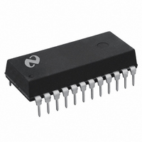
... Microprocessor compatible (8-bit data bus) Y Milliseconds through month counters Y Connection Diagrams Dual-In-Line Package Top View Order Number MM58167BN See NS Package Number N24A TRI-STATE is a registered trademark of National Semiconductor Corporation C 1995 National Semiconductor Corporation TL F 11070 56 bits of RAM with comparator to compare the real Y ...
Page 2
... Absolute Maximum Ratings If Military Aerospace specified devices are required please contact the National Semiconductor Sales Office Distributors for availability and specifications Voltage at All Pins Operating Temperature Electrical Characteristics V Parameter Supply Voltage V Outputs Enabled DD V POWER DOWN Mode DD Supply Current I Dynamic Outputs TRI-STATE ...
Page 3
Functional Description Real Time Counter The real time counter is divided into 4-bit digits with 2 digits being accessed during any read or write cycle Each digit represents a BCD number and is defined in Table I Any unused bits ...
Page 4
Functional Description (Continued) TABLE II Clock RAM Bit Map for Alarm Interrupt Everyday Address Function Milliseconds Hundredths and Tenths of Seconds Seconds Minutes ...
Page 5
Functional Description (Continued) logical zero ) When switching V to the standby or power DD down mode the POWER DOWN input should logical zero at least 1 s before V is switched When switching DD V all ...
Page 6
Functional Description (Continued) Standby Interrupt Typical Characteristics Interrupt Timing Symbol Parameter t Status Register Clock to INTERRUPT OUTPUT INTON (Pin 13) High (Note 1) t Compare Valid to STANDBY INTERRUPT ...
Page 7
Write Cycle Timing Symbol Parameter t Address Valid to Write Strobe AW t Chip Select to Write Strobe CSW t Data Valid before Write Strobe DW t Write Strobe to Ready Strobe WRY t ...
Page 8
Typical Applications Note 5 A ground line or ground plane guard trace should be included between pins 9 and 10 to insure the oscillator is not disturbed by the address line FIGURE 5 Typical Connection Diagram Note 6 Must use ...
Page 9
... Block Diagram Physical Dimensions inches (millimeters) FIGURE 7 Molded Dual-In-Line Package (N) Order Number MM58167BN NS Package Number N24A 11070– 10 ...
Page 10
... Hong Kong Ltd 49) 0-180-530 85 86 13th Floor Straight Block a Ocean Centre 5 Canton Rd 49) 0-180-530 85 85 Tsimshatsui Kowloon a Tel ( 49) 0-180-532 78 32 Hong Kong a 49) 0-180-532 93 58 Tel (852) 2737-1600 a Tel ( 49) 0-180-534 16 80 Fax (852) 2736-9960 a National Semiconductor Japan Ltd Tel 81-043-299-2309 Fax 81-043-299-2408 ...