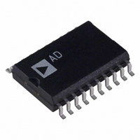
AD73311LAR-REEL7 Analog Devices Inc, AD73311LAR-REEL7 Datasheet - Page 25

AD73311LAR-REEL7
Manufacturer Part Number
AD73311LAR-REEL7
Description
IC ANALOG FRONT END 20-SOIC T/R
Manufacturer
Analog Devices Inc
Datasheet
1.AD73311LAR.pdf
(36 pages)
Specifications of AD73311LAR-REEL7
Rohs Status
RoHS non-compliant
Number Of Bits
16
Number Of Channels
2
Power (watts)
50mW
Voltage - Supply, Analog
3V
Voltage - Supply, Digital
3V
Package / Case
20-SOIC (7.5mm Width)
Single Supply Voltage (min)
2.7V
Single Supply Voltage (max)
3.3V
Package Type
SOIC W
Lead Free Status / RoHS Status
Not Compliant
Cascade Operation
Where it is required to configure a cascade of up to eight
devices, it is necessary to ensure that the timing of the SE and
RESET signals are synchronized at each device in the cascade.
A simple D-type flip-flop is sufficient to sync each signal to the
master clock MCLK, as in Figure 36.
Connection of a cascade of devices to a DSP, as shown in Fig-
ure 37, is no more complicated than connecting a single device.
Instead of connecting the SDO and SDOFS to the DSP’s Rx
port, these are now daisy-chained to the SDI and SDIFS of the
next device in the cascade. The SDO and SDOFS of the final
device in the cascade are connected to the DSP’s Rx port to
DSP CONTROL
TO SE
MCLK
DSP CONTROL
TO RESET
MCLK
TMS320C5x
ADSP-218x
DSP
DSP
CLK
CLK
D
D
TFS
DT
SCLK
DR
RFS
FL0
FL1
CLKX
CLKR
FSX
DT
DR
FSR
XF
74HC74
74HC74
RESET
1/2
1/2
Q
Q
SE SIGNAL SYNCHRONIZED
TO MCLK
RESET SIGNAL SYNCHRONIZED
TO MCLK
SDOFS
RESET
SDOFS
RESET
SDIFS
SCLK
SDIFS
SDO
SCLK
SDO
SDI
SE
SDI
SE
AD73311L
AD73311L
CODEC
CODEC
complete the cascade. SE and RESET on all devices are fed
from the signals that were synchronized with the MCLK using
the circuit as described above. The SCLK from only one device
need be connected to the DSP’s SCLK input(s) as all devices
will be running at the same SCLK frequency and phase.
Grounding and Layout
Since the analog inputs to the AD73311L are differential, most
of the voltages in the analog modulator are common-mode
voltages. The excellent common-mode rejection of the part will
remove common-mode noise on these inputs. The analog and
digital supplies of the AD73311L are independent and separately
pinned out to minimize coupling between analog and digital
sections of the device. The digital filters on the encoder section
will provide rejection of broadband noise on the power supplies,
except at integer multiples of the modulator sampling frequency.
The digital filters also remove noise from the analog inputs
provided the noise source does not saturate the analog modula-
tor. However, because the resolution of the AD73311’s ADC is
high, and the noise levels from the AD73311L are so low, care
must be taken with regard to grounding and layout.
The printed circuit board that houses the AD73311L should be
designed so the analog and digital sections are separated and
confined to certain sections of the board. The AD73311L pin
configuration offers a major advantage in that its analog and
digital interfaces are connected on opposite sides of the package.
This facilitates the use of ground planes that can be easily
separated, as shown in Figure 38. A minimum etch technique
is generally best for ground planes as it gives the best shielding.
Digital and analog ground planes should be joined in only one
place. If this connection is close to the device, it is recommended
to use a ferrite bead inductor as shown in Figure 38.
FL0
ADSP-218x
DSP
FL1
D1
D2
SCLK
TFS
DT
DR
RFS
74HC74
Q1
Q2
SDOFS
SDOFS
SDIFS
SCLK
SCLK
SDIFS
SDO
SDO
SDI
SDI
AD73311L
AD73311L
CODEC
CODEC
DEVICE 1
DEVICE 2
AD73311L
MCLK
SE
RESET
MCLK
SE
RESET


