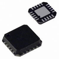
AD7699BCPZ Analog Devices Inc, AD7699BCPZ Datasheet - Page 16

AD7699BCPZ
Manufacturer Part Number
AD7699BCPZ
Description
IC ADC 8CH 16BIT 500KSPS 20LFCSP
Manufacturer
Analog Devices Inc
Datasheet
1.AD7699BCPZ.pdf
(28 pages)
Specifications of AD7699BCPZ
Data Interface
DSP, MICROWIRE™, QSPI™, Serial, SPI™
Number Of Bits
16
Sampling Rate (per Second)
500k
Number Of Converters
1
Power Dissipation (max)
32mW
Voltage Supply Source
Single Supply
Operating Temperature
-40°C ~ 85°C
Mounting Type
Surface Mount
Package / Case
20-VFQFN, CSP Exposed Pad
Resolution (bits)
16bit
Sampling Rate
500kSPS
Input Channel Type
Pseudo Differential, Single Ended
Supply Voltage Range - Analog
4.5V To 5.5V
Lead Free Status / RoHS Status
Lead free / RoHS Compliant
Available stocks
Company
Part Number
Manufacturer
Quantity
Price
Company:
Part Number:
AD7699BCPZ
Manufacturer:
ADI
Quantity:
490
Part Number:
AD7699BCPZ
Manufacturer:
ADI/亚德诺
Quantity:
20 000
AD7699
Unipolar or Bipolar
Figure 27 shows an example of the recommended connection
diagram for the AD7699 when multiple supplies are available.
Bipolar Single Supply
Figure 28 shows an example of a system with a bipolar input
using single supplies with the internal reference (optional
different VIO supply). This circuit is also useful when the
amplifier/signal conditioning circuit is remotely located with
some common mode present. Note that for any input config-
uration, the inputs, INx, are unipolar and always referenced to
GND (no negative voltages even in bipolar range).
For this circuit, a rail-to-rail input/output amplifier can be used;
however, the offset voltage vs. input common-mode range should
be noted and taken into consideration (1 LSB = 62.5 μV with
V
complement format when using the bipolar input configuration.
Refer to the AN-581 Application Note, Biasing and Decoupling
Op Amps in Single Supply Applications, at
additional details about using single-supply amplifiers.
ANALOG INPUTS
Input Structure
Figure 29 shows an equivalent circuit of the input structure of
the AD7699. The two diodes, D1 and D2, provide ESD
protection for the analog inputs, IN[7:0] and COM. Care must
be taken to ensure that the analog input signal does not exceed
the supply rails by more than 0.3 V because this causes the
diodes to become forward-biased and to start conducting
current.
These diodes can handle a forward-biased current of 130 mA
maximum. For instance, these conditions may eventually occur
when the input buffer supplies are different from VDD. In such
a case, for example, an input buffer with a short circuit, the
current limitation can be used to protect the part.
This analog input structure allows the sampling of the true
differential signal between INx+ and COM or INx+ and INx−.
(COM or INx− = GND ± 0.1 V or V
differential inputs, signals common to both inputs are rejected,
as shown in Figure 30.
REF
OR COM
OR INx–
= 4.096 V). Note that the conversion results are in twos
GND
INx+
Figure 29. Equivalent Analog Input Circuit
C
PIN
VDD
D1
D2
REF
± 0.1 V). By using these
R
www.analog.com
IN
C
IN
for
Rev. 0 | Page 16 of 28
During the acquisition phase, the impedance of the analog inputs
can be modeled as a parallel combination of the capacitor, C
and the network formed by the series connection of R
C
when the one-pole filter is active) and is a lumped component
made up of serial resistors and the on resistance of the switches.
C
Selectable Low-Pass Filter
During the conversion phase, where the switches are opened,
the input impedance is limited to C
acquiring, R
reduces undesirable aliasing effects and limits the noise from
the driving circuitry. The low-pass filter can be programmed
for the full bandwidth or ¼ of the bandwidth with CFG[6], as
shown in Table 8. Note that the converter throughput must also be
reduced by ¼ when using the filter. If the maximum throughput
is used with the BW set to ¼, the acquisition time of the
converter, t
Input Configurations
Figure 31 shows the different methods for configuring the analog
inputs with the configuration register (CFG[12:10]). Refer to
the Configuration Register, CFG section for more details.
PIN
IN
is typically 27 pF and is mainly the ADC sampling capacitor.
is primarily the pin capacitance. R
70
65
60
55
50
45
40
35
30
1
ACQ
IN
Figure 30. Analog Input CMRR vs. Frequency
and C
, is violated, resulting in poor THD.
IN
10
make a one-pole, low-pass filter that
FREQUENCY (kHz)
100
PIN
IN
. While the AD7699 is
is typically 400 Ω (8.8 kΩ
1k
IN
10k
and C
PIN
IN
,
.


