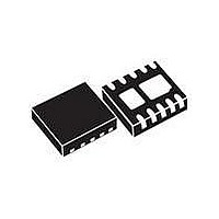
MAX11102ATB+T Maxim Integrated Products, MAX11102ATB+T Datasheet - Page 12

MAX11102ATB+T
Manufacturer Part Number
MAX11102ATB+T
Description
IC ADC 12BIT SPI/SRL 10TDFN
Manufacturer
Maxim Integrated Products
Datasheet
1.MAX11117AUTT.pdf
(30 pages)
Specifications of MAX11102ATB+T
Number Of Bits
12
Sampling Rate (per Second)
2M
Data Interface
MICROWIRE™, QSPI™, Serial, SPI™
Number Of Converters
1
Power Dissipation (max)
1.95W
Voltage Supply Source
Single Supply
Operating Temperature
-40°C ~ 125°C
Mounting Type
Surface Mount
Package / Case
10-WFDFN Exposed Pad
Conversion Rate
2 MSPs
Resolution
12 bit
Interface Type
Serial (3-Wire, SPI, QSPI, Microwire)
Snr
73 dB
Voltage Reference
1 V
Supply Voltage (max)
3.6 V
Supply Voltage (min)
2.2 V
Maximum Power Dissipation
1951 mW
Maximum Operating Temperature
+ 125 C
Mounting Style
SMD/SMT
Input Voltage
2.2 V to 3.6 V
Minimum Operating Temperature
- 40 C
Lead Free Status / RoHS Status
Lead free / RoHS Compliant
Other names
MAX11102ATB+TTR
2Msps/3Msps, Low-Power,
Serial 12-/10-/8-Bit ADCs
ELECTRICAL CHARACTERISTICS (MAX11111) (continued)
(V
unless otherwise noted. Typical values are at T
12
DIGITAL INPUTS (SCLK, CS)
Digital Input High Voltage
Digital Input Low Voltage
Digital Input Hysteresis
Digital Input Leakage Current
Digital Input Capacitance
DIGITAL OUTPUT (DOUT)
Output High Voltage
Output Low Voltage
High-Impedance Leakage
Current
High-Impedance Output
Capacitance
POWER SUPPLY
Positive Supply Voltage
Digital I/O Supply Voltage
Positive Supply Current
(Full-Power Mode)
Positive Supply Current
(Full-Power Mode), No Clock
Power-Down Current
Line Rejection
TIMING CHARACTERISTICS (Note 1)
Quiet Time
CS Pulse Width
CS Fall to SCLK Setup
CS Falling Until DOUT High-
Impedance Disabled
Data Access Time After SCLK
Falling Edge (Figure 2)
SCLK Pulse Width Low
SCLK Pulse Width High
Data Hold Time From SCLK
Falling Edge
SCLK Falling Until DOUT High-
Impedance
Power-Up Time
DD
_____________________________________________________________________________________
= 2.2V to 3.6V, V
PARAMETER
REF
= V
DD
, V
OVDD
SYMBOL
V
V
I
C
OVDD
I
I
V
V
OVDD
V
HYST
C
V
I
VDD
VDD
I
V
OUT
I
OL
PD
t
t
t
t
t
t
t
t
t
OH
DD
OL
IL
Q
IH
1
2
3
4
5
6
7
8
IL
IN
= V
DD
A
, f
= +25NC.)
Inputs at GND or V
I
I
V
V
Leakage only
V
(Note 2)
V
V
Percentage of clock period
Percentage of clock period
Figure 3
Figure 4 (Note 2)
Conversion cycle
SOURCE
SINK
AIN_
AIN_
DD
OVDD
OVDD
SCLK
= +2.2V to +3.6V, V
= 200µA (Note 2)
= V
= V
= 48MHz, 50% duty cycle, 3Msps, C
= 2.2V - 3.6V
= 1.5V - 2.2V
= 200µA (Note 2)
GND
GND
CONDITIONS
DD
REF
= 2.2V
DOUT
V
V
0.75 x
0.85 x
MIN
OVDD
OVDD
2.2
1.5
2.5
10
40
40
4
5
1
5
= 10pF, T
V
0.15 x
0.001
TYP
1.98
0.17
OVDD
1.3
2
4
A
= -40NC to +125NC,
V
V
0.25 x
0.15 x
MAX
Q1.0
OVDD
OVDD
V
0.33
16.5
3.6
3.3
Q1
10
15
60
60
14
DD
1
UNITS
LSB/V
Cycle
mA
mA
FA
FA
FA
pF
pF
ns
ns
ns
ns
ns
ns
ns
%
%
V
V
V
V
V
V
V


