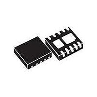
MAX11102ATB+T Maxim Integrated Products, MAX11102ATB+T Datasheet - Page 6

MAX11102ATB+T
Manufacturer Part Number
MAX11102ATB+T
Description
IC ADC 12BIT SPI/SRL 10TDFN
Manufacturer
Maxim Integrated Products
Datasheet
1.MAX11117AUTT.pdf
(30 pages)
Specifications of MAX11102ATB+T
Number Of Bits
12
Sampling Rate (per Second)
2M
Data Interface
MICROWIRE™, QSPI™, Serial, SPI™
Number Of Converters
1
Power Dissipation (max)
1.95W
Voltage Supply Source
Single Supply
Operating Temperature
-40°C ~ 125°C
Mounting Type
Surface Mount
Package / Case
10-WFDFN Exposed Pad
Conversion Rate
2 MSPs
Resolution
12 bit
Interface Type
Serial (3-Wire, SPI, QSPI, Microwire)
Snr
73 dB
Voltage Reference
1 V
Supply Voltage (max)
3.6 V
Supply Voltage (min)
2.2 V
Maximum Power Dissipation
1951 mW
Maximum Operating Temperature
+ 125 C
Mounting Style
SMD/SMT
Input Voltage
2.2 V to 3.6 V
Minimum Operating Temperature
- 40 C
Lead Free Status / RoHS Status
Lead free / RoHS Compliant
Other names
MAX11102ATB+TTR
ELECTRICAL CHARACTERISTICS (MAX11106)
(V
unless otherwise noted. Typical values are at T
2Msps/3Msps, Low-Power,
Serial 12-/10-/8-Bit ADCs
ELECTRICAL CHARACTERISTICS (MAX11105) (continued)
(V
values are at T
6
Positive Supply Current (Full-
Power Mode), No Clock
Power-Down Current
Line Rejection
TIMING CHARACTERISTICS (Note 1)
Quiet Time
CS Pulse Width
CS Fall to SCLK Setup
CS Falling Until DOUT High-
Impedance Disabled
Data Access Time After SCLK
Falling Edge
SCLK Pulse Width Low
SCLK Pulse Width High
Data Hold Time From SCLK
Falling Edge
SCLK Falling Until DOUT High-
Impedance
Power-Up Time
DC ACCURACY
Resolution
Integral Nonlinearity
Differential Nonlinearity
Offset Error
Gain Error
Total Unadjusted Error
Channel-to-Channel Offset
Matching
Channel-to-Channel Gain
Matching
DYNAMIC PERFORMANCE
Signal-to-Noise and Distortion
Signal-to-Noise Ratio
Total Harmonic Distortion
Spurious-Free Dynamic Range
DD
DD
______________________________________________________________________________________
= 2.2V to 3.6V, f
= 2.2V to 3.6V, V
PARAMETER
PARAMETER
A
= +25NC.)
SCLK
REF
= 32MHz, 50% duty cycle, 2Msps, C
= V
DD
, V
OVDD
SYMBOL
SYMBOL
SINAD
SFDR
I
DNL
SNR
THD
TUE
VDD
INL
I
OE
GE
t
PD
t
t
t
t
t
t
t
t
Q
1
2
3
4
5
6
7
8
= V
DD
A
, f
Leakage only
V
(Note 2)
Figure 2, V
Percentage of clock period
Percentage of clock period
Figure 3
Figure 4 (Note 2)
Conversion cycle
= +25NC.)
No missing codes
Excluding offset and reference errors
f
f
f
f
AIN_
AIN_
AIN_
AIN_
DD
SCLK
= +2.2V to +3.6V
= 1MHz
= 1MHz
= 1MHz
= 1MHz
= 48MHz, 50% duty cycle, 3Msps; C
DD
DOUT
= +2.2V to +3.6V
CONDITIONS
CONDITIONS
= 10pF, T
A
= -40NC to +125NC, unless otherwise noted. Typical
DOUT
MIN
MIN
2.5
10
40
40
10
61
61
75
4
5
1
5
= 10pF, T
Q0.05
Q0.05
Q0.5
Q0.5
TYP
1.48
TYP
61.8
61.8
-83
1.3
0.7
0
A
= -40NC to +125NC,
MAX
MAX
Q0.4
Q0.4
-74
Q1
Q1
10
15
60
60
14
1
UNITS
UNITS
LSB/V
Cycle
LSB
LSB
LSB
LSB
LSB
LSB
LSB
Bits
mA
dB
dB
dB
dB
FA
ns
ns
ns
ns
ns
ns
ns
%
%


