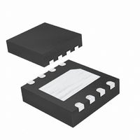
MAX1289ETA+T Maxim Integrated Products, MAX1289ETA+T Datasheet - Page 10

MAX1289ETA+T
Manufacturer Part Number
MAX1289ETA+T
Description
IC ADC 12BIT 150KSPS 8-TDFN
Manufacturer
Maxim Integrated Products
Datasheet
1.MAX1289ETAT.pdf
(15 pages)
Specifications of MAX1289ETA+T
Number Of Bits
12
Sampling Rate (per Second)
150k
Data Interface
MICROWIRE™, QSPI™, Serial, SPI™
Number Of Converters
1
Voltage Supply Source
Single Supply
Operating Temperature
-40°C ~ 85°C
Mounting Type
Surface Mount
Package / Case
8-WDFN Exposed Pad
Number Of Adc Inputs
1
Architecture
SAR
Conversion Rate
150 KSPs
Resolution
12 bit
Input Type
Voltage
Interface Type
Serial
Voltage Reference
External
Supply Voltage (max)
3.3 V
Maximum Power Dissipation
1481 mW
Maximum Operating Temperature
+ 85 C
Mounting Style
SMD/SMT
Minimum Operating Temperature
- 40 C
Lead Free Status / RoHS Status
Lead free / RoHS Compliant
Other names
MAX1289ETA+T
150ksps, 12-Bit, 2-Channel Single-Ended, and
1-Channel True-Differential ADCs
Figures 5a and 5b illustrate the conversion timing for the
MAX1286–MAX1289. The 12-bit conversion result is out-
put in MSB-first format. Data on DOUT transitions
on the falling edge of SCLK. All 12 bits must be clocked
out before CNVST transitions again. For the MAX1288/
MAX1289, data is straight binary for unipolar mode and
two’s complement for bipolar mode. For the MAX1286/
MAX1287, data is always straight binary.
Figure 6 shows the unipolar transfer function for the
MAX1286–MAX1289. Figure 7 shows the bipolar transfer
function for the MAX1288/MAX1289. Code transitions
occur halfway between successive-integer LSB values.
With CNVST low, the MAX1286–MAX1289 default to an
AutoShutdown state (< 0.2µA) after power-up and
between conversions. After detecting a rising edge on
CNVST, the part powers up, sets DOUT low, and enters
track mode. After detecting a falling edge on CNVST, the
device enters hold mode and begins the conversion. A
maximum of 3.7µs later, the device completes conver-
sion, enters shutdown, and MSB is available at DOUT.
Figure 6. Unipolar Transfer Function
10
11 . . . 111
11 . . . 110
00 . . . 011
00 . . . 010
11 . . . 101
00 . . . 001
00 . . . 000
______________________________________________________________________________________
OUTPUT CODE
0
1
Applications Information
2
INPUT VOLTAGE (LSB)
3
Automatic Shutdown Mode
FULL-SCALE
TRANSITION
Output Data Format
Transfer Function
FS - 3/2 LSB
MAX1286–
MAX1289
1 LSB =
FS = V
ZS = GND
FS
REF
4096
V
REF
An external reference is required for the MAX1286–
MAX1289. Use a 0.1µF bypass capacitor for best per-
formance. The reference input structure allows a volt-
age range of +1V to V
The MAX1286–MAX1289 feature a serial interface that is
fully compatible with SPI, QSPI, and MICROWIRE. If a
serial interface is available, establish the CPU’s serial
interface as a master, so that the CPU generates the seri-
al clock for the ADCs. Select a clock frequency up to
8MHz.
1)
2)
3)
4)
Figure 7. Bipolar Transfer Function
*V
COM
011 . . . 111
011 . . . 110
000 . . . 010
000 . . . 001
000 . . . 000
111 . . . 111
111 . . . 110
111 . . . 101
100 . . . 001
100 . . . 000
Use a general-purpose I/O line on the CPU to hold
CNVST low between conversions.
Drive CNVST high to acquire AIN1(MAX1286/
MAX1287) or unipolar mode (MAX1288/MAX1289).
To acquire AIN2 (MAX1286/MAX1287) or bipolar
mode (MAX1288/MAX1289), drive CNVST low and
high again.
Hold CNVST high for 1.4µs.
Drive CNVST low and wait approximately 3.7µs for
conversion to complete. After 3.7µs, the MSB is
available at DOUT.
≤
OUTPUT CODE
V
REF
/ 2 *V
Connection to Standard Interfaces
1 LSB =
ZS = 0
-FS =
FS =
- FS
IN
= (AIN+) - (AIN-)
-V
V
How to Perform a Conversion
REF
4096
2
V
2
REF
REF
DD
+ 50mV.
INPUT VOLTAGE (LSB)
External Reference
0
MAX1288/MAX1289
+FS - 1 LSB


