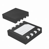
MAX1289ETA+T Maxim Integrated Products, MAX1289ETA+T Datasheet - Page 2

MAX1289ETA+T
Manufacturer Part Number
MAX1289ETA+T
Description
IC ADC 12BIT 150KSPS 8-TDFN
Manufacturer
Maxim Integrated Products
Datasheet
1.MAX1289ETAT.pdf
(15 pages)
Specifications of MAX1289ETA+T
Number Of Bits
12
Sampling Rate (per Second)
150k
Data Interface
MICROWIRE™, QSPI™, Serial, SPI™
Number Of Converters
1
Voltage Supply Source
Single Supply
Operating Temperature
-40°C ~ 85°C
Mounting Type
Surface Mount
Package / Case
8-WDFN Exposed Pad
Number Of Adc Inputs
1
Architecture
SAR
Conversion Rate
150 KSPs
Resolution
12 bit
Input Type
Voltage
Interface Type
Serial
Voltage Reference
External
Supply Voltage (max)
3.3 V
Maximum Power Dissipation
1481 mW
Maximum Operating Temperature
+ 85 C
Mounting Style
SMD/SMT
Minimum Operating Temperature
- 40 C
Lead Free Status / RoHS Status
Lead free / RoHS Compliant
Other names
MAX1289ETA+T
ABSOLUTE MAXIMUM RATINGS
V
CNVST, SCLK, DOUT to GND....................-0.3V to (V
REF, AIN1 (AIN+), AIN2 (AIN-) to GND......-0.3V to (V
Maximum Current into Any Pin............................................50mA
Continuous Power Dissipation (T
150ksps, 12-Bit, 2-Channel Single-Ended, and
1-Channel True-Differential ADCs
ELECTRICAL CHARACTERISTICS
(V
0.1µF capacitor at REF, f
noted. Typical values at T
2
Stresses beyond those listed under “Absolute Maximum Ratings” may cause permanent damage to the device. These are stress ratings only, and functional
operation of the device at these or any other conditions beyond those indicated in the operational sections of the specifications is not implied. Exposure to
absolute maximum rating conditions for extended periods may affect device reliability.
8-Pin SOT23 (derate 9.70mW/°C above T
8-Pin TDFN (derate 18.5mW/°C above T
DD
DC ACCURACY (Note 1)
Resolution
Relative Accuracy (Note 2)
Differential Nonlinearity
Offset Error
Gain Error (Note 3)
Gain Temperature Coefficient
Offset Tem p er atur e C oeffi ci ent
Channel-to-Channel Offset Matching
Channel-to-Channel Gain Matching
Input Common-Mode Rejection
Signal to Noise Plus Distortion
Total Harmonic Distortion
(up to the 5
Spurious-Free Dynamic Range
Full-Power Bandwidth
Full-Linear Bandwidth
CONVERSION RATE
Conversion Time
T/H Acquisition Time
Aperture Delay
Aperture Jitter
Maximum Serial Clock Frequency
Duty Cycle
ANALOG INPUT
Input Voltage Range (Note 4)
DYNAMIC SPECIFICATIONS: (f
for MAX1287/MAX1289, 150ksps, f
DD
_______________________________________________________________________________________
to GND ..............................................................-0.3V to +6V
= +2.7V to +3.6V, V
PARAMETER
th
harmonic)
SCLK
A
REF
= +25°C.)
= +2.5V for MAX1287/MAX1289, or V
= 8MHz (50% duty cycle), AIN- = GND for MAX1288/MAX1289. T
A
= +70°C)
IN
SCLK
(sine-wave) = 10kHz, V
SYMBOL
A
SINAD
A
= 8MHz, (50% duty cycle) AIN- = GND for MAX1288/MAX1289)
t
SFDR
f
CMR
CONV
t
= +70°C) ...1481mW
DNL
THD
SCLK
INL
ACQ
= +70°C) ...696mW
DD
DD
No missing codes over temperature
V
-3dB point
SINAD > 68dB
Does not include t
Unipolar
Bipolar
CM
+ 0.3V)
+ 0.3V)
= 0V to V
IN
= 4.096Vp-p for MAX1286/MAX1288 or V
CONDITIONS
DD
DD
Operating Temperature Range ...........................-40°C to +85°C
Storage Temperature Range .............................-60°C to +150°C
Lead Temperature (soldering, 10s) .................................+300°C
Soldering Temperature (reflow)
; zero scale input
Lead(Pb)-Free Packages...............................................+260°C
Packages Containing Lead(Pb).....................................+240°C
ACQ
= +4.75V to +5.25V, V
REF
-V
A
= +4.096V for MAX1286/MAX1288,
MIN
REF
= T
12
30
8
0
MIN
/2
IN
to T
= 2.5V
TYP
±0.4
±0.1
±0.1
±0.1
±0.4
<50
100
-82
±2
±2
70
86
30
1
MAX,
p-p
V
unless otherwise
MAX
V
±1.0
±1.0
REF
3.7
1.4
±4
±4
70
REF
/2
ppm/°C
p p m/°C
UNITS
MHz
MHz
LSB
LSB
LSB
LSB
LSB
LSB
Bits
kHz
mV
dB
dB
dB
ps
µs
µs
ns
%
V


