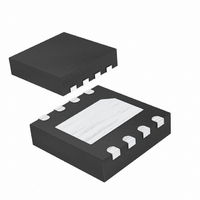
MAX1289ETA+T Maxim Integrated Products, MAX1289ETA+T Datasheet - Page 11

MAX1289ETA+T
Manufacturer Part Number
MAX1289ETA+T
Description
IC ADC 12BIT 150KSPS 8-TDFN
Manufacturer
Maxim Integrated Products
Datasheet
1.MAX1289ETAT.pdf
(15 pages)
Specifications of MAX1289ETA+T
Number Of Bits
12
Sampling Rate (per Second)
150k
Data Interface
MICROWIRE™, QSPI™, Serial, SPI™
Number Of Converters
1
Voltage Supply Source
Single Supply
Operating Temperature
-40°C ~ 85°C
Mounting Type
Surface Mount
Package / Case
8-WDFN Exposed Pad
Number Of Adc Inputs
1
Architecture
SAR
Conversion Rate
150 KSPs
Resolution
12 bit
Input Type
Voltage
Interface Type
Serial
Voltage Reference
External
Supply Voltage (max)
3.3 V
Maximum Power Dissipation
1481 mW
Maximum Operating Temperature
+ 85 C
Mounting Style
SMD/SMT
Minimum Operating Temperature
- 40 C
Lead Free Status / RoHS Status
Lead free / RoHS Compliant
Other names
MAX1289ETA+T
5)
When using an SPI (Figure 8a) or MICROWIRE inter-
face (Figures 8a and 8b), set CPOL = CPHA = 0. Two
8-bit readings are necessary to obtain the entire 12-bit
result from the ADC. DOUT data transitions on the seri-
al clock’s falling edge and is clocked into the µP on
SCLK’s rising edge. The first 8-bit data stream contains
the first 8-bits of DOUT starting with the MSB. The sec-
ond 8-bit data stream contains the remaining four result
bits. DOUT then goes high impedance.
Using the high-speed QSPI interface (Figure 9a) with
CPOL = 0 and CPHA = 0, the MAX1286–MAX1289
support a maximum f
reading is necessary to obtain the entire 12-bit result
from the ADC. DOUT data transitions on the serial
clock’s falling edge and is clocked into the µP on
Figure 8a. SPI Connections
Table 1. Detailed SSPCON Register Content
SSPOV
SSPEN
SSPM3
SSPM2
SSPM1
SSPM0
WCOL
CKP
CONTROL BIT
Activate SCLK for a minimum of 12 rising clock
edges. DOUT transitions on SCLK’s falling edge
and is available in MSB-first format. Observe the
SCLK to DOUT valid timing characteristic. Clock
data into the µP on SCLK’s rising edge.
150ksps, 12-Bit, 2-Channel Single-Ended, and
SPI
MISO
SCK
Bit 7
Bit 6
Bit 5
Bit 4
Bit 3
Bit 2
Bit 1
Bit 0
I/O
SS
SPI and MICROWIRE Interface
______________________________________________________________________________________
V
SCLK
DD
MAX1286–MAX1289
of 8MHz. One 12- to 16-bit
SETTINGS
X
X
1
0
0
0
0
1
CNVST
SCLK
DOUT
1-Channel True-Differential ADCs
QSPI Interface
MAX1286–
MAX1289
Write Collision Detection Bit
Receive Overflow Detect Bit
Synchronous Serial Port Enable Bit:
0: Disables serial port and configures these pins as I/O port pins.
1: E nab l es ser i al p or t and confi g ur es S C K, S D O, and S C I p i ns as ser i al p or t p i ns.
Clock Polarity Select Bit. CKP = 0 for SPI master mode selection.
Synchronous Serial Port Mode Select Bit. Sets SPI master mode and selects
F
CLK
= f
SYNCHRONOUS SERIAL PORT CONTROL REGISTER (SSPCON)
OSC
/ 16.
SCLK’s rising edge. The first 12 bits are the data.
DOUT then goes high impedance (Figure 9b).
The MAX1286–MAX1289 are compatible with a
PIC16/PIC17 µC, using the synchronous serial port
(SSP) module
To establish SPI communication, connect the controller
as shown in Figure 10a and configure the PIC16/PIC17
as system master. This is done by initializing its syn-
chronous serial port control register (SSPCON) and
synchronous serial port status register (SSPSTAT) to
the bit patterns shown in Tables 1 and 2.
In SPI mode, the PIC16/PIC17 µCs allow 8 bits of data
to be synchronously transmitted and received simulta-
neously. Two consecutive 8-bit readings (Figure 10b)
are necessary to obtain the entire 12-bit result from the
ADC. DOUT data transitions on the serial clock’s falling
edge and is clocked into the µC on SCLK’s rising edge.
The first 8-bit data stream contains the first 8 data bits
starting with the MSB. The second data stream con-
tains the remaining bits, D3 through D0.
Figure 8b. MICROWIRE Connections
MICROWIRE
I/O
SK
SI
PIC16 and SSP Module and
PIC17 Interface
CNVST
SCLK
DOUT
MAX1286–
MAX1289
11


