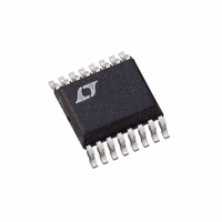
LTC2435CGN Linear Technology, LTC2435CGN Datasheet - Page 10

LTC2435CGN
Manufacturer Part Number
LTC2435CGN
Description
IC ADC DIFF I/REF 20BIT 16-SSOP
Manufacturer
Linear Technology
Datasheet
1.LTC2435-1CGN.pdf
(40 pages)
Specifications of LTC2435CGN
Number Of Bits
20
Sampling Rate (per Second)
15
Data Interface
MICROWIRE™, Serial, SPI™
Number Of Converters
2
Power Dissipation (max)
1mW
Voltage Supply Source
Single Supply
Operating Temperature
0°C ~ 70°C
Mounting Type
Surface Mount
Package / Case
16-SSOP (0.150", 3.90mm Width)
Lead Free Status / RoHS Status
Contains lead / RoHS non-compliant
Available stocks
Company
Part Number
Manufacturer
Quantity
Price
Company:
Part Number:
LTC2435CGN
Manufacturer:
LT
Quantity:
10 000
Part Number:
LTC2435CGN
Manufacturer:
LTNEAR
Quantity:
20 000
Part Number:
LTC2435CGN#PBF
Manufacturer:
LINEAR/凌特
Quantity:
20 000
PI FU CTIO S
LTC2435/LTC2435-1
GND (Pins 1, 7, 8, 9, 10, 15, 16): Ground. Multiple ground
pins internally connected for optimum ground current flow
and V
ground plane through a low impedance connection. All seven
pins must be connected to ground for proper operation.
V
(Pin 1) with a 10μF tantalum capacitor in parallel with
0.1μF ceramic capacitor as close to the part as possible.
REF
The voltage on these pins can have any value between GND
and V
maintained more positive than the reference negative
input, REF
IN
voltage on these pins can have any value between
GND – 0.3V and V
converter bipolar input range (V
from – 0.5 • (V
the converter produces unique overrange and underrange
output codes.
CS (Pin 11): Active LOW Digital Input. A LOW on this pin
enables the SDO digital output and wakes up the ADC.
Following each conversion, the ADC automatically enters
the Sleep mode and remains in this low power state as
long as CS is HIGH. A LOW-to-HIGH transition on CS
during the Data Output transfer aborts the data transfer
and starts a new conversion.
10
CC
+
U
+
(Pin 5), IN
(Pin 2): Positive Supply Voltage. Bypass to GND
CC
(Pin 3), REF
CC
decoupling. Connect each one of these pins to a
as long as the reference positive input, REF
U
–
, by at least 0.1V.
REF
–
) to 0.5 • (V
(Pin 6): Differential Analog Input. The
–
(Pin 4): Differential Reference Input.
CC
U
+ 0.3V. Within these limits the
REF
). Outside this input range
IN
= IN
+
– IN
–
) extends
+
, is
SDO (Pin 12): Three-State Digital Output. During the Data
Output period, this pin is used as serial data output. When
the chip select CS is HIGH (CS = V
high impedance state. During the Conversion and Sleep
periods, this pin is used as the conversion status output.
The conversion status can be observed by pulling CS LOW.
SCK (Pin 13): Bidirectional Digital Clock Pin. In Internal
Serial Clock Operation mode, SCK is used as digital output
for the internal serial interface clock during the Data
Output period. In External Serial Clock Operation mode,
SCK is used as digital input for the external serial interface
clock during the Data Output period. A weak internal pull-
up is automatically activated in Internal Serial Clock Op-
eration mode. The Serial Clock Operation mode is deter-
mined by the logic level applied to the SCK pin at power up
or during the most recent falling edge of CS.
F
controls the ADC’s notch frequencies and conversion
time. When the F
the converter uses its internal oscillator and the digital
filter first null is located at 50Hz. When the F
connected to GND (F
oscillator and the digital filter first null is located at 60Hz
(LTC2435) or simultaneous 50Hz/60Hz (LTC2435-1).
When F
frequency f
system clock and the digital filter first null is located at a
frequency f
O
(Pin 14): Frequency Control Pin. Digital input that
O
is driven by an external clock signal with a
EOSC
EOSC
/2560.
O
, the converter uses this signal as its
pin is connected to V
O
= OV), the converter uses its internal
CC
) the SDO pin is in a
CC
(LTC2435 only),
O
pin is
24351fb


