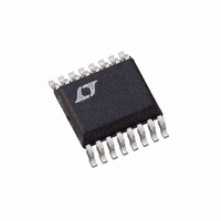
LTC2435CGN Linear Technology, LTC2435CGN Datasheet - Page 12

LTC2435CGN
Manufacturer Part Number
LTC2435CGN
Description
IC ADC DIFF I/REF 20BIT 16-SSOP
Manufacturer
Linear Technology
Datasheet
1.LTC2435-1CGN.pdf
(40 pages)
Specifications of LTC2435CGN
Number Of Bits
20
Sampling Rate (per Second)
15
Data Interface
MICROWIRE™, Serial, SPI™
Number Of Converters
2
Power Dissipation (max)
1mW
Voltage Supply Source
Single Supply
Operating Temperature
0°C ~ 70°C
Mounting Type
Surface Mount
Package / Case
16-SSOP (0.150", 3.90mm Width)
Lead Free Status / RoHS Status
Contains lead / RoHS non-compliant
Available stocks
Company
Part Number
Manufacturer
Quantity
Price
Company:
Part Number:
LTC2435CGN
Manufacturer:
LT
Quantity:
10 000
Part Number:
LTC2435CGN
Manufacturer:
LTNEAR
Quantity:
20 000
Part Number:
LTC2435CGN#PBF
Manufacturer:
LINEAR/凌特
Quantity:
20 000
APPLICATIO S I FOR ATIO
LTC2435/LTC2435-1
CONVERTER OPERATION
Converter Operation Cycle
The LTC2435/LTC2435-1 are low power, delta-sigma ana-
log-to-digital converters with an easy to use 3-wire serial
interface (see Figure 1). Their operation is made up of
three states. The converter operating cycle begins with the
conversion, followed by the sleep state and ends with the
data output (see Figure 2). The 3-wire interface consists of
serial data output (SDO), serial clock (SCK) and chip select
(CS).
Initially, the LTC2435/LTC2435-1 perform a conversion.
Once the conversion is complete, the device enters the
sleep state. While in this sleep state, power consumption
is reduced by an order of magnitude if CS is HIGH. The part
remains in the sleep state as long as CS is HIGH. The
conversion result is held indefinitely in a static shift
register while the converter is in the sleep state.
Once CS is pulled LOW, the device exits the low power
sleep mode and enters the data output state. If CS is pulled
HIGH before the first rising edge of SCK, the device returns
to the sleep mode and the conversion result is still held in
the internal static shift register. If CS remains LOW after
the first rising edge of SCK, the device begins outputting
the conversion result. Taking CS HIGH at this point will
terminate the data output state and start a new conversion.
12
Figure 2. LTC2435 State Transition Diagram
U
FALSE
U
DATA OUTPUT
CONVERT
CS = LOW
SCK
SLEEP
AND
TRUE
2435 F02
W
U
There is no latency in the conversion result. The data
output corresponds to the conversion just performed.
This result is shifted out on the serial data out pin (SDO)
under the control of the serial clock (SCK). Data is updated
on the falling edge of SCK allowing the user to reliably latch
data on the rising edge of SCK (see Figure 3). The data
output state is concluded once 24 bits are read out of the
ADC or when CS is brought HIGH. The device automati-
cally initiates a new conversion and the cycle repeats.
Through timing control of the CS and SCK pins, the
LTC2435/LTC2435-1 offer several flexible modes of op-
eration (internal or external SCK and free-running conver-
sion modes). These various modes do not require pro-
gramming configuration registers; moreover, they do not
disturb the cyclic operation described above. These modes
of operation are described in detail in the Serial Interface
Timing Modes section.
Conversion Clock
A major advantage the delta-sigma converter offers over
conventional type converters is an on-chip digital filter
(commonly implemented as a Sinc or Comb filter). For
high resolution, low frequency applications, this filter is
typically designed to reject line frequencies of 50Hz or
60Hz plus their harmonics. The filter rejection perfor-
mance is directly related to the accuracy of the converter
system clock. The LTC2435/LTC2435-1 incorporate a
highly accurate on-chip oscillator. This eliminates the
need for external frequency setting components such as
crystals or oscillators. Clocked by the on-chip oscillator,
the LTC2435 achieves a minimum of 110dB rejection at
the line frequency (50Hz or 60Hz ±2%), while the
LTC2435-1 achieves a minimum of 87db rejection at 50Hz
±2% and 60Hz ±2% simultaneously.
Ease of Use
The LTC2435/LTC2435-1 data output has no latency,
filter settling delay or redundant data associated with the
conversion cycle. There is a one-to-one correspondence
between the conversion and the output data. Therefore,
multiplexing multiple analog voltages is easy.
24351fb


