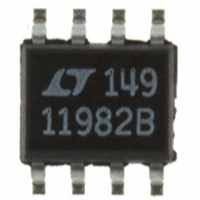
LTC1198-2BCS8 Linear Technology, LTC1198-2BCS8 Datasheet - Page 15

LTC1198-2BCS8
Manufacturer Part Number
LTC1198-2BCS8
Description
IC ADC 8BIT 750KHZ SAMPL 8-SOIC
Manufacturer
Linear Technology
Datasheet
1.LTC1196-2BCS8PBF.pdf
(28 pages)
Specifications of LTC1198-2BCS8
Number Of Bits
8
Sampling Rate (per Second)
750k
Data Interface
Serial
Number Of Converters
1
Power Dissipation (max)
50mW
Voltage Supply Source
Single Supply
Operating Temperature
0°C ~ 70°C
Mounting Type
Surface Mount
Package / Case
8-SOIC (0.154", 3.90mm Width)
Lead Free Status / RoHS Status
Contains lead / RoHS non-compliant
Available stocks
Company
Part Number
Manufacturer
Quantity
Price
Company:
Part Number:
LTC1198-2BCS8
Manufacturer:
LT
Quantity:
10 000
Part Number:
LTC1198-2BCS8
Manufacturer:
LTC
Quantity:
20 000
Part Number:
LTC1198-2BCS8#PBF
Manufacturer:
LINEAR/凌特
Quantity:
20 000
APPLICATIONS INFORMATION
ADDRESS IN
Connection to a microprocessor or a DSP serial port is
quite simple (see the Data Transfer section). It requires no
additional hardware, but the speed will be limited by the
clock rate of the microprocessor or the DSP which limits
the conversion time of the LTC1196/LTC1198.
Data Transfer
Data transfer differs slightly between the LTC1196 and
the LTC1198. The LTC1196 interfaces over three lines:
CS, CLK and D
depicted by the LTC1196 Operating Sequence in Figure 1.
After CS falls, the fi rst CLK pulse enables D
null bits, the A/D conversion result is output on the D
line. Bringing CS HIGH resets the LTC1196 for the next
data exchange.
The LTC1198 can transfer data with three or four wires.
The additional input, D
MUX confi guration.
The data transfer between the LTC1198 and the digital
systems can be broken into two sections: Input Data
Word and A/D Conversion Result. First, each bit of the
input data word is captured on the rising CLK edge by the
LTC1198. Second, each bit of the A/D conversion result
on the D
LTC1198. This bit should be captured on the next rising
CLK edge by the digital systems (see the A/D Conversion
Result section).
Data transfer is initiated by a falling chip select (CS) signal
as depicted by the LTC1198 Operating Sequence in Figure 2.
After CS falls, the LTC1198 looks for a START bit. After
the START bit is received, the 4-bit input word is shifted
into the D
confi gure the LTC1198. The last two bits of the input word
allow the ADC to acquire the input voltage by 2.5 clocks
before the conversion starts. After the conversion starts,
SHIFT MUX
CS
OUT
IN
D
IN1
line is updated on the rising CLK edge by the
2 NULL BITS
input. The fi rst two bits of the input word
OUT
. A falling CS initiates data transfer as
D
OUT1
IN
SHIFT A/D CONVERSION
RESULT OUT
, is used to select the 2-channel
D
IN2
OUT
D
OUT2
. After two
1196/98 AI01
OUT
START Bit
The fi rst logical one clocked into the D
goes LOW is the START bit. The START bit initiates the data
transfer. The LTC1198 will ignore all leading zeros which
precede this logical one . After the START bit is received,
the remaining bits of the input word will be clocked in.
Further inputs on the D
next CS cycle.
Multiplexer (MUX) Address
The two bits of the input word following the START bit as-
sign the MUX confi guration for the requested conversion.
For a given channel selection, the converter will measure
the voltage between the two channels indicated by the “+”
and “–” signs in the selected row of the following table.
In single-ended mode, all input channels are measured
with respect to GND.
two null bits and the conversion result are output on the
D
brought HIGH. This resets the LTC1198 in preparation for
the next data exchange.
Input Data Word
The LTC1196 requires no D
fi gured to have a single differential input. The conversion
result is output on the D
followed by zeros indefi nitely if clocks are continuously
applied with CS LOW.
The LTC1198 clocks data into the D
ing edge of the clock. The input data word is defi ned as
follows:
OUT
SINGLE-ENDED
DIFFERENTIAL
line. At the end of the data exchange CS should be
MUX MODE
MUX MODE
START
SGL/DIFF
LTC1198 Channel Selection
MUX ADDRESS
1
1
0
0
LTC1196/LTC1198
SGL/
DIFF
ADDRESS
OUT
MUX
IN
ODD/SIGN
ODD/
SIGN
IN
pin are then ignored until the
0
1
0
1
line in an MSB-fi rst sequence,
word. It is permanently con-
DUMMY
CHANNEL #
0
+
+
–
DUMMY
BITS
DUMMY
IN
119698 AI02
input on the ris-
IN
1
+
–
+
1196/98 AI03
input after CS
GND
–
–
15
119698fb


