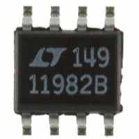
LTC1198-2BCS8 Linear Technology, LTC1198-2BCS8 Datasheet - Page 21

LTC1198-2BCS8
Manufacturer Part Number
LTC1198-2BCS8
Description
IC ADC 8BIT 750KHZ SAMPL 8-SOIC
Manufacturer
Linear Technology
Datasheet
1.LTC1196-2BCS8PBF.pdf
(28 pages)
Specifications of LTC1198-2BCS8
Number Of Bits
8
Sampling Rate (per Second)
750k
Data Interface
Serial
Number Of Converters
1
Power Dissipation (max)
50mW
Voltage Supply Source
Single Supply
Operating Temperature
0°C ~ 70°C
Mounting Type
Surface Mount
Package / Case
8-SOIC (0.154", 3.90mm Width)
Lead Free Status / RoHS Status
Contains lead / RoHS non-compliant
Available stocks
Company
Part Number
Manufacturer
Quantity
Price
Company:
Part Number:
LTC1198-2BCS8
Manufacturer:
LT
Quantity:
10 000
Part Number:
LTC1198-2BCS8
Manufacturer:
LTC
Quantity:
20 000
Part Number:
LTC1198-2BCS8#PBF
Manufacturer:
LINEAR/凌特
Quantity:
20 000
APPLICATIONS INFORMATION
Noise with Reduced V
The total input referred noise of the LTC1196 can be
reduced to approximately 2mV
good bypassing, good layout techniques and minimizing
noise on the reference inputs. This noise is insignifi cant
with a 5V reference but will become a larger fraction of
an LSB as the size of the LSB is reduced.
For operation with a 5V reference, the 2mV noise is only
0.1LSB peak-to-peak. In this case, the LTC1196 noise
will contribute virtually no uncertainty to the output code.
However, for reduced references, the noise may become
a signifi cant fraction of an LSB and cause undesirable jit-
ter in the output code. For example, with a 1V reference,
this same 2mV noise is 0.5LSB peak-to-peak. This will
reduce the range of input voltages over which a stable
output code can be achieved by 1LSB. If the reference is
further reduced to 200mV, the 2mV noise becomes equal
to 2.5LSB and a stable code is diffi cult to achieve. In this
case averaging readings is necessary.
This noise data was taken in a very clean setup. Any setup
induced noise (noise or ripple on V
add to the internal noise. The lower the reference voltage
to be used, the more critical it becomes to have a clean,
noise-free setup.
REF
P-P
using a ground plane,
CC
, V
Figure 10. LTC1196 Nonaveraged, 4096 Point FFT Plot
REF
–100
–10
–20
–30
–40
–50
–60
–70
–80
–90
or V
0
0
IN
) will
100
FREQUENCY (kHz)
200
DYNAMIC PERFORMANCE
The LTC1196/LTC1198 have exceptionally high speed
sampling capability. Fast Fourier Transform (FFT) test
techniques are used to characterize the ADC’s frequency
response, distortion and noise at the rated throughput. By
applying a low distortion sine wave and analyzing the digital
output using a FFT algorithm, the ADC’s spectral content
can be examined for frequencies outside the fundamental.
Figure 10 shows a typical LTC1196 FFT plot.
Signal-to-Noise Ratio
The Signal-to-Noise plus Distortion Ratio [S/(N + D)] is
the ratio between the RMS amplitude of the fundamental
input frequency to the RMS amplitude of all other frequency
components at the ADC’s output. The output is band limited
to frequencies above DC and below one half the sampling
frequency. Figure 10 shows a typical spectral content with
a 882kHz sampling rate.
Effective Number of Bits
The Effective Number of Bits (ENOBs) is a measurement
of the resolution of an ADC and is directly related to
S/(N + D) by the equation:
N = [S/(N + D) –1.76]/6.02
300
V
f
f
IN
SMPL
CC
= 29kHz
= 5V
400
= 882kHz
1196/98 G25
500
LTC1196/LTC1198
21
119698fb


