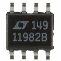
LTC1198-2BCS8 Linear Technology, LTC1198-2BCS8 Datasheet - Page 18

LTC1198-2BCS8
Manufacturer Part Number
LTC1198-2BCS8
Description
IC ADC 8BIT 750KHZ SAMPL 8-SOIC
Manufacturer
Linear Technology
Datasheet
1.LTC1196-2BCS8PBF.pdf
(28 pages)
Specifications of LTC1198-2BCS8
Number Of Bits
8
Sampling Rate (per Second)
750k
Data Interface
Serial
Number Of Converters
1
Power Dissipation (max)
50mW
Voltage Supply Source
Single Supply
Operating Temperature
0°C ~ 70°C
Mounting Type
Surface Mount
Package / Case
8-SOIC (0.154", 3.90mm Width)
Lead Free Status / RoHS Status
Contains lead / RoHS non-compliant
Available stocks
Company
Part Number
Manufacturer
Quantity
Price
Company:
Part Number:
LTC1198-2BCS8
Manufacturer:
LT
Quantity:
10 000
Part Number:
LTC1198-2BCS8
Manufacturer:
LTC
Quantity:
20 000
Part Number:
LTC1198-2BCS8#PBF
Manufacturer:
LINEAR/凌特
Quantity:
20 000
LTC1196/LTC1198
APPLICATIONS INFORMATION
Mixed Supplies
It is possible to have a digital system running off a 5V supply
and communicate with the LTC1196/LTC1198 operating on
a 3V supply. Achieving this reduces the outputs of D
from the ADCs to toggle the equivalent input of the digital
system. The CS, CLK and D
5V signals from the digital system without causing any
problem (see the Digital Input Logic Threshold vs Supply
Voltage curve in the Typical Performance Characteristics
section). With the LTC1196 operating on a 3V supply, the
output of D
easily meets TTL levels (see Figure 6).
18
COMMON MODE RANGE
DIFFERENTIAL INPUTS
Figure 6. Interfacing a 3V Powered LTC1196 to a 5V System
+ INPUT
– INPUT
0V TO 3V
OUT
D
CLK
OUT
D
CS
IN
only goes between 0V and 3V. This signal
CS
+IN
–IN
GND
LTC1196
D
IN
V
CLK
V
OUT
REF
CC
START
inputs of the ADCs will take
3V
3V
4.7μF
Figure 7. LTC1198 “+” and “–” Input Settling Windows
SGL/DIFF
P1.4
P1.3
P1.2
(e.g., 8051)
MPU
1196/98 F06
ODD/SIGN
S
1ST BIT TEST:
– INPUT MUST SETTLE DURING THIS TIME
A
M
P
OUT
5V
E L
DUMMY
SETTLE DURING
BOARD LAYOUT CONSIDERATIONS
Grounding and Bypassing
The LTC1196/LTC1198 are easy to use if some care is
taken. They should be used with an analog ground plane
and single-point grounding techniques. The GND pin
should be tied directly to the ground plane.
The V
1μF tantalum with leads as short as possible. If the power
supply is clean, the LTC1196/LTC1198 can also operate
with smaller 0.1μF surface mount or ceramic bypass ca-
pacitors. All analog inputs should be referenced directly to
the single-point ground. Digital inputs and outputs should
be shielded from and/or routed away from the reference
and analog circuitry.
SAMPLE-AND-HOLD
Both the LTC1196 and the LTC1198 provide a built-in
sample-and-hold (S&H) function to acquire the input
signal. The S&H acquires the input signal from “+” input
during t
LTC1198 can sample input signals in either single-ended
or differential mode (see Figure 7).
+ INPUT MUST
THIS TIME
t
SMPL
CC
SMPL
pin should be bypassed to the ground plane with a
DUMMY
as shown in Figures 1 and 2. The S&H of the
H
O
L
D
t
CONV
DON’T CARE
B7
1196/98 F07
119698fb


