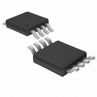
LTC1864LACMS8#TR Linear Technology, LTC1864LACMS8#TR Datasheet - Page 7

LTC1864LACMS8#TR
Manufacturer Part Number
LTC1864LACMS8#TR
Description
IC ADC 16-BIT 1CH 150KSPS 8-MSOP
Manufacturer
Linear Technology
Datasheet
1.LTC1865LCMSPBF.pdf
(16 pages)
Specifications of LTC1864LACMS8#TR
Number Of Bits
16
Sampling Rate (per Second)
150k
Data Interface
MICROWIRE™, Serial, SPI™
Number Of Converters
1
Power Dissipation (max)
400mW
Voltage Supply Source
Single Supply
Operating Temperature
0°C ~ 70°C
Mounting Type
Surface Mount
Package / Case
8-TSSOP, 8-MSOP (0.118", 3.00mm Width)
Lead Free Status / RoHS Status
Contains lead / RoHS non-compliant
Available stocks
Company
Part Number
Manufacturer
Quantity
Price
LTC1864L
LTC1865L (MSOP Package)
LTC1865L (SO-8 Package)
CONV (Pin 1): Convert Input. A logic high on this input
starts the A/D conversion process. If the CONV input is left
high after the A/D conversion is finished, the part powers
down. A logic low on this input enables the SDO pin,
allowing the data to be shifted out.
CH0, CH1 (Pins 2, 3): Analog Inputs. These inputs must
be free of noise with respect to GND.
GND (Pin 4): Analog Ground. GND should be tied directly
to an analog ground plane.
PI FU CTIO S
V
the span of the A/D converter and must be kept free of
noise with respect to GND.
IN
free of noise with respect to GND.
GND (Pin 4): Analog Ground. GND should be tied directly
to an analog ground plane.
CONV (Pin 5): Convert Input. A logic high on this input
starts the A/D conversion process. If the CONV input is left
high after the A/D conversion is finished, the part powers
CONV (Pin 1): Convert Input. A logic high on this input
starts the A/D conversion process. If the CONV input is left
high after the A/D conversion is finished, the part powers
down. A logic low on this input enables the SDO pin,
allowing the data to be shifted out.
CH0, CH1 (Pins 2, 3): Analog Inputs. These inputs must
be free of noise with respect to AGND.
AGND (Pin 4): Analog Ground. AGND should be tied
directly to an analog ground plane.
DGND (Pin 5): Digital Ground. DGND should be tied
directly to an analog ground plane.
SDI (Pin 6): Digital Data Input. The A/D configuration
word is shifted into this input.
REF
+
U
, IN
(Pin 1): Reference Input. The reference input defines
–
(Pins 2, 3): Analog Inputs. These inputs must be
U
U
down. A logic low on this input enables the SDO pin,
allowing the data to be shifted out.
SDO (Pin 6): Digital Data Output. The A/D conversion
result is shifted out of this pin.
SCK (Pin 7): Shift Clock Input. This clock synchronizes the
serial data transfer.
V
free of noise and ripple by bypassing directly to the
analog ground plane.
SDO (Pin 7): Digital Data Output. The A/D conversion
result is shifted out of this output.
SCK (Pin 8): Shift Clock Input. This clock synchronizes the
serial data transfer.
V
free of noise and ripple by bypassing directly to the
analog ground plane.
V
fines the span of the A/D converter and must be kept free
of noise with respect to AGND.
SDI (Pin 5): Digital Data Input. The A/D configuration
word is shifted into this input.
SDO (Pin 6): Digital Data Output. The A/D conversion
result is shifted out of this output.
SCK (Pin 7): Shift Clock Input. This clock synchronizes the
serial data transfer.
V
free of noise and ripple by bypassing directly to the
analog ground plane. V
CC
CC
REF
CC
(Pin 8): Positive Supply. This supply must be kept
(Pin 9): Positive Supply. This supply must be kept
(Pin 8): Positive Supply. This supply must be kept
(Pin 10): Reference Input. The reference input de-
LTC1864L/LTC1865L
REF
is tied internally to this pin.
sn18645L 18645Lfs
7


