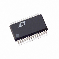
LTC2418CGN#TRPBF Linear Technology, LTC2418CGN#TRPBF Datasheet - Page 29

LTC2418CGN#TRPBF
Manufacturer Part Number
LTC2418CGN#TRPBF
Description
IC ADC 24BIT DIFF INPUT 28SSOP
Manufacturer
Linear Technology
Datasheet
1.LTC2418CGNPBF.pdf
(48 pages)
Specifications of LTC2418CGN#TRPBF
Number Of Bits
24
Sampling Rate (per Second)
7.5
Data Interface
MICROWIRE™, Serial, SPI™
Number Of Converters
1
Power Dissipation (max)
1mW
Voltage Supply Source
Single Supply
Operating Temperature
0°C ~ 70°C
Mounting Type
Surface Mount
Package / Case
28-SSOP (0.150", 3.95mm Width)
Lead Free Status / RoHS Status
Lead free / RoHS Compliant
Available stocks
Company
Part Number
Manufacturer
Quantity
Price
APPLICATIO S I FOR ATIO
values for C
gain performance without significant benefits of reference
filtering and the user is advised to avoid them.
Larger values of reference capacitors (C
be required as reference filters in certain configurations.
Such capacitors will average the reference sampling charge
and the external source resistance will see a quasi con-
stant reference differential impedance. When F
(internal oscillator and 60Hz notch), the typical differential
reference resistance is 1.3MΩ which will generate a gain
error of approximately 0.38ppm for each ohm of source
resistance driving REF
oscillator and 50Hz notch), the typical differential refer-
ence resistance is 1.56MΩ which will generate a gain error
Figure 20. +FS Error vs R
Figure 18. +FS Error vs R
–180
–270
–360
–450
–90
–10
–20
–30
–40
–50
REF
0
0
0 100 200 300 400 500 600 700 800 900 1000
1
V
REF
REF
IN
IN
F
T
will deteriorate the converter offset and
V
REF
REF
IN
IN
F
T
O
A
CC
O
A
CC
+
–
+
–
= GND
= 25°C
= GND
= 25°C
+
–
= 3.75V
= 1.25V
+
= 3.75V
= 5V
–
= 1.25V
C
= 5V
U
C
10
= 5V
= GND
REF
= 5V
= GND
C
REF
REF
+
C
= 0.001µF
REF
SOURCE
= 0.01µF
or REF
= 100pF
SOURCE
R
R
= 0pF
100
U
SOURCE
SOURCE
at REF
C
–
REF
at REF
. When F
(Ω)
(Ω)
1k
C
= 1µF, 10µF
C
REF
REF
W
+
+
= 0.01µF
and REF
= 0.1µF
10k
or REF
REF
O
2414/18 F20
2414/18 F18
= HIGH (internal
> 0.01µF) may
100k
–
–
(Small C
(Large C
U
O
= LOW
IN
REF
)
)
of approximately 0.32ppm for each ohm of source resis-
tance driving REF
external oscillator with a frequency f
sion clock operation), the typical differential reference
resistance is 0.20 • 10
resistance driving REF
2.47 • 10
resistance on the two reference pins is additive with
respect to this gain error. The typical +FS and –FS errors
for various combinations of source resistance seen by the
REF
nected to these pins are shown in Figures 18, 19, 20
and 21.
Figure 21. –FS Error vs R
Figure 19. –FS Error vs R
+
and REF
–6
• f
450
360
270
180
90
50
40
30
20
10
EOSC
0
0
–
0 100 200 300 400 500 600 700 800 900 1000
1
pins and external capacitance C
V
REF
REF
IN
IN
F
T
V
REF
REF
IN
IN
F
T
ppm gain error. The effect of the source
O
O
CC
A
A
+
CC
+
+
–
–
= GND
= 25°C
= GND
= 25°C
+
–
= 1.25V
= 3.75V
+
–
= 1.25V
= 5V
LTC2414/LTC2418
C
= 5V
= 3.75V
or REF
C
10
= 5V
= GND
REF
= 5V
= GND
C
REF
12
REF
SOURCE
C
= 0.001µF
REF
/f
SOURCE
= 0.01µF
= 100pF
EOSC
R
= 0pF
R
100
SOURCE
+
SOURCE
–
. When F
at REF
or REF
Ω and each ohm of source
at REF
C
REF
(Ω)
(Ω)
C
1k
REF
= 1µF, 10µF
EOSC
+
C
REF
= 0.01µF
+
and REF
or REF
O
–
10k
= 0.1µF
(external conver-
is driven by an
2414/18 F21
2414/18 F19
will result in
–
–
100k
(Small C
(Large C
REF
29
241418fa
con-
IN
REF
)
)


