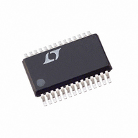
LTC2418CGN#TRPBF Linear Technology, LTC2418CGN#TRPBF Datasheet - Page 35

LTC2418CGN#TRPBF
Manufacturer Part Number
LTC2418CGN#TRPBF
Description
IC ADC 24BIT DIFF INPUT 28SSOP
Manufacturer
Linear Technology
Datasheet
1.LTC2418CGNPBF.pdf
(48 pages)
Specifications of LTC2418CGN#TRPBF
Number Of Bits
24
Sampling Rate (per Second)
7.5
Data Interface
MICROWIRE™, Serial, SPI™
Number Of Converters
1
Power Dissipation (max)
1mW
Voltage Supply Source
Single Supply
Operating Temperature
0°C ~ 70°C
Mounting Type
Surface Mount
Package / Case
28-SSOP (0.150", 3.95mm Width)
Lead Free Status / RoHS Status
Lead free / RoHS Compliant
Available stocks
Company
Part Number
Manufacturer
Quantity
Price
APPLICATIO S I FOR ATIO
Traditional high order delta-sigma modulators, while
providing very good linearity and resolution, suffer from
potential instabilities at large input signal levels. The pro-
prietary architecture used for the LTC2414/LTC2418 third
order modulator resolves this problem and guarantees a
predictable stable behavior at input signal levels of up to
150% of full scale. In many industrial applications, it is not
uncommon to have to measure microvolt level signals
superimposed over volt level perturbations and LTC2414/
LTC2418 is eminently suited for such tasks. When the
perturbation is differential, the specification of interest is
the normal mode rejection for large input signal levels.
With a reference voltage V
has a full-scale differential input range of 5V peak-to-peak.
Figure 39. Measured Input Normal Mode Rejection vs Input Frequency with Input Perturbation of 150% Full Scale (60Hz Notch)
Figure 40. Measured Input Normal Mode Rejection vs Input Frequency with Input Perturbation of 150% Full Scale (50Hz Notch)
U
REF
U
–100
–120
–100
–120
– 60
–20
–40
–80
–20
–40
– 60
–80
= 5V, the LTC2414/LTC2418
0
0
0
0
12.5 25 37.5 50 62.5 75 87.5 100 112.5 125 137.5 150 162.5 175 187.5 200
15
W
30
45
60
U
75
90
INPUT FREQUENCY (Hz)
INPUT FREQUENCY (Hz)
105 120 135 150 165 180 195 210 225 240
Figures 39 and 40 show measurement results for the
LTC2414/LTC2418 normal mode rejection ratio with a 7.5V
peak-to-peak (150% of full scale) input signal superim-
posed over the more traditional normal mode rejection
ratio results obtained with a 5V peak-to-peak (full scale)
input signal. In Figure 39, the LTC2414/LTC2418 uses the
internal oscillator with the notch set at 60Hz (F
and in Figure 40 it uses the internal oscillator with the
notch set at 50Hz (F
LTC2418 rejection performance is maintained with no com-
promises in this extreme situation. When operating with
large input signal levels, the user must observe that such
signals do not violate the device absolute maximum
ratings.
V
V
(150% OF FULL SCALE)
V
V
(150% OF FULL SCALE)
IN(P-P)
IN(P-P)
IN(P-P)
IN(P-P)
= 5V
= 7.5V
= 5V
= 7.5V
O
V
REF
REF
V
SDI = GND
F
T
LTC2414/LTC2418
V
REF
REF
V
SDI = GND
F
T
= HIGH). It is clear that the LTC2414/
O
A
CC
INCM
O
A
CC
INCM
= 5V
= 25°C
= GND
= 25°C
+
= 5V
–
+
–
= 5V
= 5V
= GND
= 5V
= GND
= 2.5V
= 2.5V
2414/18 F40
2414/18 F39
O
= LOW)
35
241418fa


