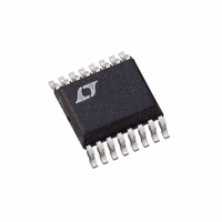
LTC1402IGN Linear Technology, LTC1402IGN Datasheet - Page 4

LTC1402IGN
Manufacturer Part Number
LTC1402IGN
Description
IC ADC 12BIT 2.2MSPS SHDN 16SSOP
Manufacturer
Linear Technology
Datasheet
1.LTC1402CGNPBF.pdf
(24 pages)
Specifications of LTC1402IGN
Number Of Bits
12
Sampling Rate (per Second)
2.2M
Data Interface
MICROWIRE™, Serial, SPI™
Number Of Converters
1
Power Dissipation (max)
150mW
Voltage Supply Source
Analog and Digital, Dual ±
Operating Temperature
-40°C ~ 85°C
Mounting Type
Surface Mount
Package / Case
16-SSOP (0.150", 3.90mm Width)
Lead Free Status / RoHS Status
Contains lead / RoHS non-compliant
Available stocks
Company
Part Number
Manufacturer
Quantity
Price
Company:
Part Number:
LTC1402IGN
Manufacturer:
NEC
Quantity:
6 945
Part Number:
LTC1402IGN#PBF
Manufacturer:
LINEAR/凌特
Quantity:
20 000
Part Number:
LTC1402IGN#TRPBF
Manufacturer:
LINEAR/凌特
Quantity:
20 000
POWER REQUIRE E TS
LTC1402
TI I G CHARACTERISTICS
range, otherwise specifications are at T
range, otherwise specifications are at T
SYMBOL
V
V
I
I
PD
SYMBOL
f
t
t
t
t
t
t
t
t
t
t
t
t
t
t
t
t
t
Note 1: Absolute Maximum Ratings are those values beyond which the life
of a device may be impaired.
Note 2: All voltage values are with respect to ground with DGND, AGND1
and AGND2 wired together.
Note 3: When these pins are taken below V
clamped by internal diodes. This product can handle input currents greater
than 100mA below V
Note 4: When these pins are taken below V
internal diodes. This product can handle input currents greater than
100mA below V
Note 5: V
specifications and V
4
DD
SS
SAMPLE(MAX)
THROUGHPUT
SCK
CONV
0
1
2
3
4
5
6
7
8
8a
9
10
11
12
DD
SS
W
DD
U
= 5V, f
PARAMETER
Positive Supply Voltage
Negative Supply Voltage
Positive Supply Current
Negative Supply Current
Power Dissipation
SS
PARAMETER
Maximum Sampling Frequency (Conversion Rate)
Minimum Sampling Period (Conversion + Acquisiton Period)
Minimum Clock Period
Conversion Time
14th SCLK to CONV Interval
Minimum Positive or Negative SCK Pulse Width
CONV to SCK Setup Time
SCK After CONV
Minimum Positive or Negative CONV Pulse Width
SCK to Sample Mode
CONV to Hold Mode
Minimum Delay Between Conversions
Minimum Delay from SCK to Valid Bits 0 Through 11
Minimum Delay from SCK to Valid REFREADY
SCK to Hi-Z at D
Previous D
REFREADY Bit Delay After Sleep-to-Wake Transition
V
REF
or greater than V
SAMPLE
SS
SS
Settling Time After Sleep-to-Wake Transition
= – 5V for bipolar specifications.
or greater than V
= 2.2MHz, V
OUT
Bit Remains Valid After SCK
OUT
DD
W U
. These pins are not clamped to V
SS
DD
= 0V for unipolar mode
SS
SS
without latchup.
, they will be clamped by
A
A
or above V
= 25 C. (Note 5)
= 25 C. (Note 5)
The
CONDITIONS
Active Mode
Nap Mode
Sleep Mode
Active, Sleep or Nap Modes with SCK Off
Active Mode with SCK in Fixed State (Hi or Lo)
DD
, they will be
The
denotes the specifications which apply over the full operating temperature
denotes the specifications which apply over the full operating temperature
DD
.
CONDITIONS
(Note 9)
(Notes 9, 10, 16)
(Note 9)
(Notes 9, 13)
(Note 9)
(Note 9)
(Note 9)
(Notes 9, 14)
(Note 9)
(Notes 9, 15)
(Notes 9, 15)
(Notes 9, 15)
(Notes 9, 15)
(Notes 9, 17)
(Notes 9, 17)
Note 6: Linearity, offset and full-scale specifications apply for a single-
ended A
bipolar mode with 5V supplies.
Note 7: Integral linearity is defined as the deviation of a code from the
straight line passing through the actual endpoints of a transfer curve. The
deviation is measured from the center of quantization band.
Note 8: Bipolar offset is the offset measured from – 0.5LSB when the input
flickers between 1000 0000 0000 and 0111 1111 1111.
Note 9: Guaranteed by design, not subject to test.
Note 10: Recommended operating conditions.
Note 11: The analog input range is defined as the voltage difference
between A
with a single 5V supply if the absolute voltages of the inputs remain within
the single 5V supply voltage.
IN
+
IN
input with A
+
and A
IN
–
. The bipolar 2.048V input range could be used
IN
–
grounded and using the internal reference in
MIN
2.2
28
57
48
0
4
– 5.25
MIN
4.75
11.4
TYP
3.8
7.3
3.5
3.4
14
15
10
9
9
7
2
TYP
18
90
3
2
10000
MAX
455
12
14
12
20
16
6
5
5
MAX
5.25
150
30
10
0
5
2
SCK cycles
UNITS
UNITS
MHz
mW
mA
mA
ms
ms
ns
ns
ns
ns
ns
ns
ns
ns
ns
ns
ns
ns
ns
ns
V
V
A
A


