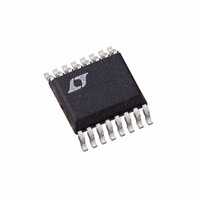
LTC1402IGN Linear Technology, LTC1402IGN Datasheet - Page 8

LTC1402IGN
Manufacturer Part Number
LTC1402IGN
Description
IC ADC 12BIT 2.2MSPS SHDN 16SSOP
Manufacturer
Linear Technology
Datasheet
1.LTC1402CGNPBF.pdf
(24 pages)
Specifications of LTC1402IGN
Number Of Bits
12
Sampling Rate (per Second)
2.2M
Data Interface
MICROWIRE™, Serial, SPI™
Number Of Converters
1
Power Dissipation (max)
150mW
Voltage Supply Source
Analog and Digital, Dual ±
Operating Temperature
-40°C ~ 85°C
Mounting Type
Surface Mount
Package / Case
16-SSOP (0.150", 3.90mm Width)
Lead Free Status / RoHS Status
Contains lead / RoHS non-compliant
Available stocks
Company
Part Number
Manufacturer
Quantity
Price
Company:
Part Number:
LTC1402IGN
Manufacturer:
NEC
Quantity:
6 945
Part Number:
LTC1402IGN#PBF
Manufacturer:
LINEAR/凌特
Quantity:
20 000
Part Number:
LTC1402IGN#TRPBF
Manufacturer:
LINEAR/凌特
Quantity:
20 000
LTC1402
PIN
GAIN (Pin 7): Tie to AGND2 to set the reference voltage to
4.096V or tie to V
(Note 4)
BIP/UNI (Pin 8): Tie to logic low to set the input range to
unipolar mode or tie to logic high to set the input range to
bipolar mode. (Note 4)
OGND (Pin 9): Output Ground for the Output Driver. This
pin can be tied to the digital ground of the system. All other
ground pins should be tied to the analog ground plane.
D
output data word represents the analog input at the start
of the previous conversion.
OV
driving 5V logic. Tie to 3V when driving 3V logic.
DV
DGND with 10 F ceramic (or 10 F tantalum in parallel with
0.1 F ceramic).
BLOCK DIAGRA
8
OUT
DD
DD
U
(Pin 10): Three-State Data Output. (Note 3) Each
(Pin 11): Output Data Driver Power. Tie to V
(Pin 12): Digital Power for Internal Logic. Bypass to
FUNCTIONS
U
AGND2
AGND1
DGND
GAIN
V
A
A
REF
IN
IN
+
–
REF
13
3
4
7
5
6
2
to set the reference voltage to 2.048V.
U
64k
2.048V REF
W
+
–
REF AMP
64k
INTERNAL
CLOCK
DD
12-BIT CAPACITIVE DAC
SUCCESSIVE APPROXIMATION
when
C
C
CONV
SAMPLE
SAMPLE
CONTROL LOGIC
16
REGISTER
DGND (Pin 13): Digital Ground for Internal Logic. Tie to
solid analog ground plane.
V
analog ground plane with 10 F ceramic (or 10 F tantalum
in parallel with 0.1 F ceramic) or tie directly to the solid
analog ground plane for single supply use. Must be set
more negative than either A
SCK (Pin 15): External Clock. Advances the conversion
process and sequences the output data at D
rising edge. Responds to 5V or 3V CMOS and to TTL levels.
(Note 4). One or more pulses wake from Nap or Sleep.
CONV (Pin 16): Holds the input analog signal and starts
the conversion on the rising edge. Responds to 5V or 3V
CMOS and to TTL levels. (Note 4). Two pulses with SCK in
fixed high or fixed low state start Nap Mode. Four pulses
with SCK in fixed high or fixed low state start Sleep mode.
SS
SCK
(Pin 14): Negative Supply Voltage. Bypass to solid
15
ZEROING SWITCHES
+
–
COMP
OUTPUT
DRIVER
IN
+
or A
1402 BD
IN
–
1
12
14
8
10
11
9
. Set to 0V or – 5V.
AV
DV
V
BIP/UNI
D
OV
OGND
SS
OUT
DD
DD
DD
OUT
on the


