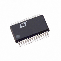
LTC1418IG Linear Technology, LTC1418IG Datasheet - Page 13

LTC1418IG
Manufacturer Part Number
LTC1418IG
Description
IC A/D CONV 14BIT SRL&PAR 28SSOP
Manufacturer
Linear Technology
Datasheet
1.LTC1418ACGPBF.pdf
(28 pages)
Specifications of LTC1418IG
Number Of Bits
14
Sampling Rate (per Second)
200k
Data Interface
Serial, Parallel
Number Of Converters
1
Power Dissipation (max)
21.5mW Unipolar; 31.5mW Bipolar
Voltage Supply Source
Dual ±
Operating Temperature
-40°C ~ 85°C
Mounting Type
Surface Mount
Package / Case
28-SSOP (0.200", 5.30mm Width)
Lead Free Status / RoHS Status
Contains lead / RoHS non-compliant
Available stocks
Company
Part Number
Manufacturer
Quantity
Price
Company:
Part Number:
LTC1418IG
Manufacturer:
LT
Quantity:
2 027
UNIPOLAR / BIPOLAR OPERATION AND ADJUSTMENT
Figure 9a shows the ideal input/output characteristics for
the LTC1418. The code transitions occur midway between
successive integer LSB values (i.e., 0.5LSB, 1.5LSB,
2.5LSB, … FS – 1.5LSB). The output code is natural binary
with 1LSB = FS/16384 = 4.096V/16384 = 250 V. Figure 9b
shows the input/output transfer characteristics for the
bipolar mode in two’s complement format.
Unipolar Offset and Full-Scale Error Adjustment
In applications where absolute accuracy is important,
offset and full-scale errors can be adjusted to zero. Offset
error must be adjusted before full-scale error. Figures
10a and 10b show the extra components required for full-
APPLICATIONS
Figure 9a. LTC1418 Unipolar Transfer Characteristics
Figure 9b. LTC1418 Bipolar Transfer Characteristics
111...111
111...110
111...101
111...100
000...011
000...010
000...001
000...000
011...111
011...110
000...001
000...000
111...111
111...110
100...001
100...000
0V
–FS/2
UNIPOLAR
ZERO
1LSB = FS
LSB
1
U
16384
INPUT VOLTAGE (V)
INPUT VOLTAGE (V)
INFORMATION
U
=
4.096V
BIPOLAR
16384
LSB
–1
ZERO
0V
FS = 4.096V
1LSB = FS/16384
LSB
1
W
FS/2 – 1LSB
FS – 1LSB
1418 F9a
1418 F9b
U
scale error adjustment. Zero offset is achieved by adjust-
ing the offset applied to the A
error apply 125 V (i.e., 0.5LSB) at the input and adjust
the offset at the A
between 0000 0000 0000 00 and 0000 0000 0000 01. For
full-scale adjustment, an input voltage of 4.095625V
(FS – 1.5LSBs) is applied to A
the output code flickers between 1111 1111 1111 10 and
1111 1111 1111 11.
Bipolar Offset and Full-Scale Error Adjustment
Bipolar offset and full-scale errors are adjusted in a similar
fashion to the unipolar case. Again, bipolar offset error
must be adjusted before full-scale error. Bipolar offset
50k
R1
Figure 10a. Offset and Full-Scale Adjust Circuit
If – 5V Is Not Available
Figure 10b. Offset and Full-Scale Adjust Circuit
If – 5V Is Available
–5V
50k
R1
*ONLY NEEDED IF V
10 F
ABOVE GROUND
R5
47k
10 F
24k
R3
R5
47k
ANALOG INPUT
ANALOG INPUT
50k
IN
R2
24k
R3
–
50k
R2
input until the output code flickers
R6
24k
100
0.1 F
R6
24k
R4
SS
100
0.1 F
GOES
R4
100
IN
R8
IN
+
–
and R2 is adjusted until
1
2
3
4
5
input. For zero offset
1N5817
A
A
V
REFCOMP
AGND V
R7
48k
1
2
3
4
5
IN
IN
REF
+
–
A
A
V
REFCOMP
AGND V
*
IN
IN
REF
+
–
LTC1418
V
–5V
5V
LTC1418
DD
SS
V
LTC1418
5V
DD
SS
1418 F10b
1418 F10a
13


