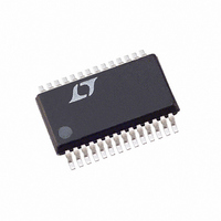
LTC1418IG Linear Technology, LTC1418IG Datasheet - Page 18

LTC1418IG
Manufacturer Part Number
LTC1418IG
Description
IC A/D CONV 14BIT SRL&PAR 28SSOP
Manufacturer
Linear Technology
Datasheet
1.LTC1418ACGPBF.pdf
(28 pages)
Specifications of LTC1418IG
Number Of Bits
14
Sampling Rate (per Second)
200k
Data Interface
Serial, Parallel
Number Of Converters
1
Power Dissipation (max)
21.5mW Unipolar; 31.5mW Bipolar
Voltage Supply Source
Dual ±
Operating Temperature
-40°C ~ 85°C
Mounting Type
Surface Mount
Package / Case
28-SSOP (0.200", 5.30mm Width)
Lead Free Status / RoHS Status
Contains lead / RoHS non-compliant
Available stocks
Company
Part Number
Manufacturer
Quantity
Price
Company:
Part Number:
LTC1418IG
Manufacturer:
LT
Quantity:
2 027
mode is much slower since the reference circuit must
power up and settle to 0.005% for full 14-bit accuracy.
Sleep mode wake-up time is dependent on the value of
the capacitor connected to the REFCOMP (Pin 4). The
wake-up time is 30ms with the recommended 10 F
capacitor. Shutdown is controlled by Pin 22 (SHDN); the
ADC is in shutdown when it is low. The shutdown mode
is selected with Pin 25 (CS); low selects nap (see Figure
13b), high selects sleep.
LTC1418
APPLICATIONS
Conversion Control
Conversion start is controlled by the CS and CONVST
inputs. A falling edge of CONVST pin will start a conversion
after the ADC has been selected (i.e., CS is low, see Figure
14). Once initiated, it cannot be restarted until the conver-
sion is complete. Converter status is indicated by the
BUSY output. BUSY is low during a conversion.
Data Output
The data format is controlled by the SER/PAR input pin;
logic low selects parallel output format. In parallel mode
the 14-bit data output word D0 to D13 is updated at the end
of each conversion on Pins 6 to 13 and Pins 15 to 20. A
logic high applied to SER/PAR selects the serial formatted
data output and Pins 16 to 20 assume their serial function,
Pins 6 to 13 and 15 are in the Hi-Z state. In either parallel
18
CONVST
Figure 13a. SHDN to CONVST Wake-Up Timing
SHDN
SHDN
CS
Figure 13b. CS to SHDN Timing
U
t
4
INFORMATION
t
3
U
W
1418 F13a
1418 F13b
U
or serial data formats, outputs will be active only when CS
and RD are low. Any other combination of CS and RD will
three-state the output. In unipolar mode (V
data will be in straight binary format (corresponding to the
unipolar input range). In bipolar mode (V
data will be in two’s complement format (corresponding to
the bipolar input range).
Parallel Output Mode
Parallel mode is selected with a logic 0 applied to the
SER/PAR pin. Figures 15 through 19 show different modes
of parallel output operation. In modes 1a and 1b (Figures
15 and 16) CS and RD are both tied low. The falling edge
of CONVST starts the conversion. The data outputs are
always enabled and data can be latched with the BUSY
rising edge. Mode 1a shows operation with a narrow logic
low CONVST pulse. Mode 1b shows a narrow logic high
CONVST pulse.
In mode 2 (Figure 17) CS is tied low. The falling edge of
CONVST signal again starts the conversion. Data outputs
are in three-state until read by the MPU with the RD signal.
Mode 2 can be used for operation with a shared databus.
In slow memory and ROM modes (Figures 18 and 19), CS
is tied low and CONVST and RD are tied together. The MPU
starts the conversion and reads the output with the RD
signal. Conversions are started by the MPU or DSP (no
external sample clock).
In slow memory mode the processor takes RD (= CONVST)
low and starts the conversion. BUSY goes low forcing the
processor into a wait state. The previous conversion result
appears on the data outputs. When the conversion is
complete, the new conversion results appear on the data
Figure 14. CS to CONVST Set-Up Timing
CONVST
RD
CS
t
1
t
2
1418 F14
SS
SS
= – 5V), the
= 0V) the


