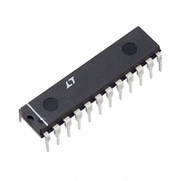
LTC1272-3CCN Linear Technology, LTC1272-3CCN Datasheet - Page 12

LTC1272-3CCN
Manufacturer Part Number
LTC1272-3CCN
Description
IC A/D CONV 12BIT SAMPLING 24DIP
Manufacturer
Linear Technology
Datasheet
1.LTC1272-3CCSW.pdf
(20 pages)
Specifications of LTC1272-3CCN
Number Of Bits
12
Sampling Rate (per Second)
250k
Data Interface
Parallel
Number Of Converters
1
Power Dissipation (max)
75mW
Voltage Supply Source
Single Supply
Operating Temperature
0°C ~ 70°C
Mounting Type
Through Hole
Package / Case
24-DIP (0.300", 7.62mm)
Lead Free Status / RoHS Status
Contains lead / RoHS non-compliant
Available stocks
Company
Part Number
Manufacturer
Quantity
Price
Company:
Part Number:
LTC1272-3CCN
Manufacturer:
LT
Quantity:
2
Part Number:
LTC1272-3CCN#PBF
Manufacturer:
LINEAR/凌特
Quantity:
20 000
There are two modes of operation as outlined by the timing
diagrams of Figures 13 to 17. Slow Memory Mode is
designed for microprocessors which can be driven into a
Wait state, a Read operation brings CS and RD low which
initiates a conversion and data is read when conversion is
complete.
A
Table 1. Data Bus Output, CS and RD = Low
Data Outputs*
HBEN = Low
HBEN = High
Note: *D11 . . . D0/8 are the ADC data output pins
LTC1272
12
PPLICATI
DB11 . . . DB0 are the 12-bit conversion results, DB11 is the MSB
PIN 4
DB11
DB11
D11
O
U
S
PIN 5
DB10
DB10
D10
CS & RD
*
I FOR ATIO
CLK IN
UNCERTAIN CONVERSION TIME FOR 30ns < t
THE LTC1272 IS ALSO COMPATIBLE WITH THE AD7572 SYNCHRONIZATION MODES.
SEE “DIGITAL INTERFACE” TEXT.
BUSY
U
HBEN
RD
CS
Figure 12. Internal Logic for Control Inputs CS, RD and HBEN
19
21
20
PIN 6
DB9
DB9
D11....D0/8 ARE THE ADC DATA OUTPUT PINS
DB11....DB0 ARE THE 12-BIT CONVERSION RESULTS
D9
t
Figure 13. RD and CLK IN for Synchronous Operation
W
2
LTC1272
t
14
≥ 40ns*
PIN 7
DB8
DB8
D8
U
PIN 8
DB7
Low
D7
(MSB)
DB11
5V
14
< 180ns
ACTIVE HIGH
ACTIVE HIGH
D
PIN 9
DB6
Low
D6
CLEAR
BUSY
FLOP
The second is the ROM Mode which does not require
microprocessor Wait states. A Read operation brings CS
and RD low which initiates a conversion and reads the
previous conversion result.
FLIP
t
CONV
DB10
Q
PIN 10
ENABLE THREE-STATE OUTPUTS
D11....D0/8 = DB11....DB0
ENABLE THREE-STATE OUTPUTS
D11....D8 = DB11....DB8
D7....D4 = LOW
D3/11....D0/8 = DB11....DB8
DB5
Low
D5
CONVERSION START
(RISING EDGE TRIGGER)
DB1
PIN 11
DB4
Low
D4
LTC1272 • TA14
PIN 13
D3/11
DB11
DB3
(LSB)
DB0
LTC1272 • TA15
t
13
PIN 14
D2/10
DB10
DB2
PIN 15
D1/9
DB1
DB9
PIN 16
D0/8
DB0
DB8
1272fb
1272fb
1272fb


