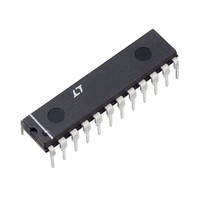
LTC1272-3CCN Linear Technology, LTC1272-3CCN Datasheet - Page 17

LTC1272-3CCN
Manufacturer Part Number
LTC1272-3CCN
Description
IC A/D CONV 12BIT SAMPLING 24DIP
Manufacturer
Linear Technology
Datasheet
1.LTC1272-3CCSW.pdf
(20 pages)
Specifications of LTC1272-3CCN
Number Of Bits
12
Sampling Rate (per Second)
250k
Data Interface
Parallel
Number Of Converters
1
Power Dissipation (max)
75mW
Voltage Supply Source
Single Supply
Operating Temperature
0°C ~ 70°C
Mounting Type
Through Hole
Package / Case
24-DIP (0.300", 7.62mm)
Lead Free Status / RoHS Status
Contains lead / RoHS non-compliant
Available stocks
Company
Part Number
Manufacturer
Quantity
Price
Company:
Part Number:
LTC1272-3CCN
Manufacturer:
LT
Quantity:
2
Part Number:
LTC1272-3CCN#PBF
Manufacturer:
LINEAR/凌特
Quantity:
20 000
A
Compatibility with the AD7572
Figure 21 shows the simple, single 5V configuration
recommended for new designs with the LTC1272. If an
AD7572 replacement or upgrade is desired, the LTC1272
can be plugged into an AD7572 socket with minor modi-
fications. It can be used as a replacement or to upgrade
with sample-and-hold, single supply operation and re-
duced power consumption.
The LTC1272, while consuming less power overall than
the AD7572, draws more current from the 5V supply (it
draws no power from the –15V supply). Also, a 1µs
PPLICATI
O
U
S
OUTPUT
I FOR ATIO
2.42V
V
U
REF
8 OR 12-BIT
Figure 21. Single 5V Supply, 3µs, 12-Bit Sampling ADC
PARALLEL
ANALOG INPUT
0.1µF
W
(0V TO 5V)
BUS
+
10µF
*
*
FOR GROUNDING AND BYPASSING HINTS
SEE FIGURE 11 AND APPLICATION HINTS
SECTION
U
D11 (MSB)
D10
D9
D8
D7
D6
D5
D4
DGND
A
V
AGND
REF
IN
LTC1272
CLK OUT
CLK IN
D2/10
BUSY
HBEN
D3/11
minimum time between conversions must be provided to
allow the sample-and-hold to reacquire the analog input.
Figure 22 shows that if the clock is synchronous with CS
and RD, it is only necessary to short out the 10Ω series
resistor and reverse the polarity of the 10µF bypass
capacitor on the V
and can be removed, or, because there is no internal
connection to pin 23, it can remain unmodified. The clock
can be considered synchronous with CS and RD in cases
where the LTC1272 CLK IN signal is derived from the same
clock as the microprocessor reading the LTC1272.
D0/8
D1/9
V
NC
RD
DD
CS
10 F
µP
CONTROL
LINES
µ
+
LTC1272 • TA03
REF
pin. The –15V supply is not required
5V
0.1 F*
µ
LTC1272
17
1272fb


